AD9219-65EBZ Analog Devices Inc, AD9219-65EBZ Datasheet - Page 34
AD9219-65EBZ
Manufacturer Part Number
AD9219-65EBZ
Description
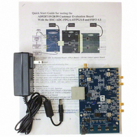
Quad 10-bit 65 MSPS Serial LVDS ADC EB
Manufacturer
Analog Devices Inc
Datasheet
1.AD9219ABCPZRL7-40.pdf
(52 pages)
Specifications of AD9219-65EBZ
Number Of Adc's
4
Number Of Bits
10
Sampling Rate (per Second)
40M
Data Interface
Serial
Inputs Per Adc
2 Single
Input Range
2 Vpp
Power (typ) @ Conditions
378mW @ 1.8 V
Voltage Supply Source
Single Supply
Operating Temperature
-40°C ~ 85°C
Utilized Ic / Part
AD9219
Lead Free Status / RoHS Status
Lead free / RoHS Compliant


AD9219
Addr.
(Hex)
14
15
16
19
1A
1B
1C
21
22
Register Name
output_mode
output_adjust
output_phase
user_patt1_lsb
user_patt1_msb
user_patt2_lsb
user_patt2_msb
serial_control
serial_ch_stat
(MSB)
Bit 7
X
X
X
B7
B15
B7
B15
LSB first
1 = on
0 = off
(default)
X
Bit 6
0 = LVDS
ANSI-644
(default)
1 = LVDS
low power
(IEEE1596.3
similar)
X
X
B6
B14
B6
B14
X
X
Bit 5
X
Output driver
termination
00 = none (default)
01 = 200 Ω
10 = 100 Ω
11 = 100 Ω
X
B5
B13
B5
B13
X
X
Rev. D | Page 34 of 52
Bit 4
X
X
B4
B12
B4
B12
X
X
Bit 3
X
X
0011 = output clock phase adjust
(0000 through 1010)
0000 = 0° relative to data edge
0001 = 60° relative to data edge
0010 = 120° relative to data edge
0011 = 180° relative to data edge (default)
0101 = 300° relative to data edge
0110 = 360° relative to data edge
1000 = 480° relative to data edge
1001 = 540° relative to data edge
1010 = 600° relative to data edge
1011 to 1111 = 660° relative to data edge
B3
B11
B3
B11
<10
MSPS,
low
encode
rate
mode
1 = on
0 = off
(default)
X
Bit 2
Output
invert
1 = on
0 = off
(default)
X
B2
B10
B2
B10
000 = 10 bits (default, normal bit
stream)
001 = 8 bits
010 = 10 bits
011 = 12 bits
100 = 14 bits
X
Bit 1
00 = offset binary
(default)
01 = twos complement
X
B1
B9
B1
B9
Channel
output
reset
1 = on
0 = off
(default)
(LSB)
Bit 0
X
Channel
power-
down
1 = on
0 = off
(default)
B0
B8
B0
B8
Default
Value
(Hex)
0x00
0x00
0x03
0x00
0x00
0x00
0x00
0x00
0x00
Default Notes/
Comments
Configures the
outputs and the
format of the data.
Determines
LVDS or other
output properties.
Primarily func-
tions to set the
LVDS span and
common-mode
levels in place of
an external
resistor.
On devices that
utilize global
clock divide,
determines
which phase of
the divider
output is used to
supply the
output clock.
Internal latching
is unaffected.
User-defined
pattern, 1 LSB.
User-defined
pattern, 1 MSB.
User-defined
pattern, 2 LSB.
User-defined
pattern, 2 MSB.
Serial stream
control. Default
causes MSB first
and the native
bit stream (global).
Used to power
down individual
sections of a
converter (local).
Related parts for AD9219-65EBZ
Image
Part Number
Description
Manufacturer
Datasheet
Request
R

Part Number:
Description:
Quad 10-bit 65 MSPS Serial LVDS ADC EB
Manufacturer:
Analog Devices Inc
Datasheet:

Part Number:
Description:
±1.7g Dual-Axis IMEMS Accelerometer Evaluation Board
Manufacturer:
Analog Devices Inc
Datasheet:
Part Number:
Description:
Inertial Sensor Evaluation System
Manufacturer:
Analog Devices Inc
Datasheet:
Part Number:
Description:
Manufacturer:
Analog Devices Inc
Datasheet:
Part Number:
Description:
Manufacturer:
Analog Devices Inc
Datasheet:
Part Number:
Description:
Manufacturer:
Analog Devices Inc
Datasheet:
Part Number:
Description:
Manufacturer:
Analog Devices Inc
Datasheet:
Part Number:
Description:
Manufacturer:
Analog Devices Inc
Datasheet:
Part Number:
Description:
Manufacturer:
Analog Devices Inc
Datasheet:
Part Number:
Description:
Manufacturer:
Analog Devices Inc
Datasheet:
Part Number:
Description:
Manufacturer:
Analog Devices Inc
Datasheet:
Part Number:
Description:
Manufacturer:
Analog Devices Inc
Datasheet:
Part Number:
Description:
Manufacturer:
Analog Devices Inc
Datasheet: