AD9219-65EBZ Analog Devices Inc, AD9219-65EBZ Datasheet
AD9219-65EBZ
Specifications of AD9219-65EBZ


Related parts for AD9219-65EBZ


AD9219-65EBZ Summary of contents
Page 1
... The available digital test patterns include built-in deterministic and pseudorandom patterns, along with custom user- defined test patterns entered via the serial port interface (SPI). The AD9219 is available in an RoHS compliant, 48-lead LFCSP specified over the industrial temperature range of −40°C to +85°C. PRODUCT HIGHLIGHTS 1 ...
Page 2
... AD9219 TABLE OF CONTENTS Features .............................................................................................. 1 Applications ....................................................................................... 1 General Description ......................................................................... 1 Functional Block Diagram .............................................................. 1 Product Highlights ........................................................................... 1 Revision History ............................................................................... 2 Specifications ..................................................................................... 3 AC Specifications .......................................................................... 4 Digital Specifications ................................................................... 5 Switching Specifications .............................................................. 6 Timing Diagrams .............................................................................. 7 Absolute Maximum Ratings ............................................................ 9 Thermal Impedance ..................................................................... 9 ESD Caution .................................................................................. 9 Pin Configuration and Function Descriptions ........................... 10 Equivalent Circuits ......................................................................... 12 Typical Performance Characteristics ........................................... 14 Theory of Operation ...................................................................... 19 REVISION HISTORY 5/10— ...
Page 3
... Full 1.7 1.8 1.9 Full 130 142 Full 30 32 Full 295 313 Full 2 5.8 Full 72 Full −100 Full −100 Rev Page AD9219 AD9219-65 Min Typ Max Unit 10 Bits Guaranteed ±1 ±8 mV ±2 ±8 mV ±2 ±3 ±0.3 ±0 ±0.15 ±0.4 LSB ±0.3 ± ...
Page 4
... Full −84 Full −82 −71 Full −80 Full −79 Full −90 Full −90 −77 Full −90 Full −88 25°C 81.5 25°C 79.5 Rev Page AD9219-65 Min Typ Max Unit 60.2 dB 60.2 dB 59.0 60.2 dB 60.1 dB 60.1 dB 60.1 dB 58.8 60.0 dB 59.8 dB 9.71 Bits 9 ...
Page 5
... Full 1.79 Full 0.05 LVDS Full 247 454 Full 1.125 1.375 Offset binary LVDS Full 150 250 Full 1.10 1.30 Offset binary Rev Page AD9219 AD9219-65 Min Typ Max Unit CMOS/LVDS/LVPECL 250 mV p-p 1 kΩ 1.5 pF 1.2 3 kΩ 0 ...
Page 6
... SAMPLE SAMPLE SAMPLE (t /20) − 300 (t /20) (t /20) + 300 SAMPLE SAMPLE SAMPLE ±50 ±150 600 375 8 500 <1 1 Rev Page AD9219-65 Min Typ Max 65 10 7.7 7.7 2.0 2.5 3.5 300 300 2.0 2.5 3 FCO (t /20) SAMPLE (t /20) − 300 ...
Page 7
... Figure 2. 10-Bit Data Serial Stream, MSB First (Default FRAME t DATA MSB D10 – – – – – – 9 Figure 3. 12-Bit Data Serial Stream, MSB First Rev Page MSB – – – – – – – MSB N – – – – – – – 8 AD9219 – 8 D10 N – 8 ...
Page 8
... AD9219 N – 1 VIN ± CLK– CLK+ t CPD DCO– DCO+ t FCO FCO– FCO – FRAME t DATA LSB – – – – – – – 9 Figure 4. 10-Bit Stream, LSB First Rev Page LSB – – – – – – – 8 ...
Page 9
... V to +3.9 V −0 +2 θ for a 4-layer PCB with solid ground plane (simulated). Exposed pad JA soldered to PCB. −0 +2.0 V −40°C to +85°C ESD CAUTION 150°C 300°C −65°C to +150°C Rev Page AD9219 θ 1 θ θ Unit °C/W 21 12.6 1.2 ° ...
Page 10
... CSB 31 PDWN PIN 1 INDICATOR EXPOSED PADDLE, PIN 0 4 (BOTTOM OF PACKAGE AD9219 TOP VIEW Figure 5. 48-Lead LFCSP Pin Configuration, Top View Description Analog Ground (Exposed Paddle) 1.8 V Analog Supply Digital Output Driver Ground 1.8 V Digital Output Driver Supply ADC D Analog Input Complement ...
Page 11
... ADC A Analog Input Complement ADC B Analog Input Complement ADC B Analog Input True External resistor sets the internal ADC core bias current Reference Mode Selection Voltage Reference Input/Output Differential Reference (Negative) Differential Reference (Positive) ADC C Analog Input True ADC C Analog Input Complement Rev Page AD9219 ...
Page 12
... AD9219 EQUIVALENT CIRCUITS VIN ± x Figure 6. Equivalent Analog Input Circuit 10Ω CLK+ 10kΩ 10kΩ 10Ω CLK– Figure 7. Equivalent Clock Input Circuit 350Ω SDIO/ODM 30kΩ Figure 8. Equivalent SDIO/ODM Input Circuit 1.25V AND PDWN Rev Page DRVDD V V D– ...
Page 13
... AVDD 70kΩ 1kΩ CSB Figure 12. Equivalent CSB Input Circuit 1kΩ SENSE Figure 13. Equivalent SENSE Circuit VREF Figure 14. Equivalent VREF Circuit Rev Page AD9219 6kΩ ...
Page 14
... AD9219 TYPICAL PERFORMANCE CHARACTERISTICS 0 –20 –40 –60 –80 –100 –120 FREQUENCY (MHz) Figure 15. Single-Tone 32k FFT with f = 2.4 MHz –20 –40 –60 –80 –100 –120 FREQUENCY (MHz) Figure 16. Single-Tone 32k FFT with MHz –20 –40 –60 –80 –100 –120 FREQUENCY (MHz) Figure 17 ...
Page 15
... MSPS Figure 25. SNR/SFDR vs. Encode, f SAMPLE Figure 26. SNR/SFDR vs. Encode MSPS SAMPLE Rev Page p-p, SFDR 2V p-p, SNR ENCODE (MSPS MHz SAMPLE 2V p-p, SFDR 2V p-p, SNR ENCODE (MSPS) = 10.3 MHz SAMPLE 2V p-p, SFDR 2V p-p, SNR ENCODE (MSPS MHz SAMPLE AD9219 MSPS MSPS MSPS ...
Page 16
... AD9219 100 10.3MHz 40MSPS SAMPLE p-p, SFDR –60 –50 –40 –30 ANALOG INPUT LEVEL (dBFS) Figure 27. SNR/SFDR vs. Analog Input Level 100 35MHz 40MSPS SAMPLE p-p, SFDR –60 –50 –40 –30 ANALOG INPUT LEVEL (dBFS) Figure 28. SNR/SFDR vs. Analog Input Level 100 10.3MHz ...
Page 17
... SAMPLE Rev Page p-p, SFDR 2V p-p, SINAD –40 – TEMPERATURE (°C) = 10.3 MHz 200 400 600 800 CODE Figure 37. INL 2.4 MHz MSPS IN SAMPLE 0 0 200 400 600 800 CODES Figure 38. DNL 2.4 MHz MSPS IN SAMPLE AD9219 MSPS SAMPLE 1000 1000 ...
Page 18
... AD9219 –45.0 –45.5 –46.0 –46.5 –47.0 –47.5 –48 FREQUENCY (MHz) Figure 39. CMRR vs. Frequency, f SAMPLE 1.2 1.0 0.8 0.6 0.4 0 – – – CODE Figure 40. Input-Referred Noise Histogram MSPS 0 LSB rms MSPS Figure 42. Full-Power Bandwidth vs. Frequency, f SAMPLE Rev Page NPR = 51.72dB NOTCH = 18.0MHz – ...
Page 19
... Wideband A/D Converters” (Volume 39, April 2005) for more information at www.analog.com. In general, the precise values depend on the application. The analog inputs of the AD9219 are not internally dc-biased. Therefore, in ac-coupled applications, the user must provide this bias externally. Setting the device so that V ...
Page 20
... AD9219 80 75 SFDR (dBc SNR (dB 0.2 0.4 0.6 0.8 ANALOG INPUT COMMON-MODE VOLTAGE (V) Figure 44. SNR/SFDR vs. Common-Mode Voltage 2.4 MHz MSPS IN SAMPLE 80 75 SFDR (dBc SNR (dB 0.2 0.4 0.6 0.8 ANALOG INPUT COMMON-MODE VOLTAGE (V) Figure 45. SNR/SFDR vs. Common-Mode Voltage MHz MSPS IN SAMPLE 1.0 1 ...
Page 21
... In the case of the AD9219, the largest input span available p-p. Differential Input Configurations There are several ways to drive the AD9219 either actively or passively; however, optimum performance is achieved by driving the analog input differentially. For example, using the ...
Page 22
... This signal is typically ac-coupled to the CLK+ and CLK− pins via a transformer or capacitors. These pins are biased internally and require no additional biasing. Figure 52 shows a preferred method for clocking the AD9219. The low jitter clock source is converted from a single-ended signal to a differential signal using an RF transformer. The back-to- back Schottky diodes across the secondary transformer limit clock excursions into the AD9219 to approximately 0 ...
Page 23
... Figure 57). The clock input should be treated as an analog signal in cases where aperture jitter may affect the dynamic range of the AD9219. Power supplies for clock drivers should be separated from the ADC output driver supplies to avoid modulating the clock signal with digital noise ...
Page 24
... AD9219 By asserting the PDWN pin high, the AD9219 is placed into power-down mode. In this state, the ADC typically dissipates 3 mW. During power-down, the LVDS output drivers are placed into a high impedance state. If any of the SPI features are changed before the power-down feature is enabled, the chip continues to function after PDWN is pulled low without requiring a reset ...
Page 25
... External 100 Ω Far Termination Only (VIN + x) − (VIN − x), Digital Output Offset Binary Input Span = 2 V p-p (V) (D9 ... D0) +1.00 1111 1111 11 0.00 1000 0000 00 −0.001953 0111 1111 11 −1.00 0000 0000 00 AD9219 1ns 150ps ...
Page 26
... AD9219 Two output clocks are provided to assist in capturing data from the AD9219. The DCO is used to clock the output data and is equal to five times the sample clock (CLK) rate. Data is clocked out of the AD9219 and must be captured on the rising and falling edges of the DCO that supports double data rate (DDR) Table 9 ...
Page 27
... Section 5.6 of the ITU-T 0.150 (05/96) standard. The only differences are that the starting value must be a specific value instead of all 1s (see Table 10 for the initial values) and the AD9219 inverts the bit stream with relation to the ITU standard. Table 10. PN Sequence Initial ...
Page 28
... Voltage Reference A stable, accurate 0.5 V voltage reference is built into the AD9219. This is gained up internally by a factor of 2, setting V to 1.0 V, which results in a full-scale differential input span REF p-p. The V VREF pin can be driven externally with a 1 ...
Page 29
... The analog input full- scale range of the ADC equals twice the voltage of the reference pin for either an internal or an external reference configuration. If the reference of the AD9219 is used to drive multiple converters to improve gain matching, the loading of the refer- ence by the other converters must be considered. Figure 66 depicts how the internal reference voltage is affected by loading ...
Page 30
... If multiple SDIO pins share a common connection, care should be taken to ensure that proper V same load for each AD9219, Figure 68 shows the number of SDIO pins that can be connected together and the resulting V level. This interface is flexible enough to be controlled by either ...
Page 31
... Minimum time for the SDIO pin to switch from an input to an output relative to the SCLK falling edge (not shown in Figure 69) Minimum time for the SDIO pin to switch from an output to an input relative to the SCLK rising edge (not shown in Figure 69) Rev Page DON’T CARE AD9219 DON’T CARE ...
Page 32
... Addresses that have values marked as 0 should be considered reserved and have a 0 written into their registers during power-up. DEFAULT VALUES When the AD9219 comes out of a reset, critical registers are preloaded with default values. These values are indicated in Table 16, where an X refers to an undefined feature. ...
Page 33
... Bit 5 Bit 4 Bit 3 Bit 2 Soft 1 1 Soft reset reset off 0 = off (default) (default) 8-bit Chip ID Bits [7:0] (AD9219 = 0x03), (default Clock Clock Data Data Channel Channel Channel Channel DCO FCO off 0 = off ...
Page 34
... AD9219 Addr. (MSB) (Hex) Register Name Bit 7 Bit 6 14 output_mode LVDS ANSI-644 (default LVDS low power (IEEE1596.3 similar) 15 output_adjust output_phase user_patt1_lsb user_patt1_msb B15 B14 1B user_patt2_lsb user_patt2_msb B15 B14 21 serial_control LSB first off (default) 22 serial_ch_stat X X Bit 5 Bit 4 Bit 3 Bit Output invert ...
Page 35
... AD9219. An exposed continuous copper plane on the PCB should mate to the AD9219 exposed paddle, Pin 0. The copper plane should have several vias to achieve the lowest possible resistive thermal path for heat dissipation to flow through the bottom of the PCB. ...
Page 36
... Figure 73 to Figure 77). Figure 71 shows the typical bench characterization setup used to evaluate the ac performance of the AD9219 critical that the signal sources used for the analog input and clock have very low phase noise (<1 ps rms jitter) to realize the optimum performance of the converter ...
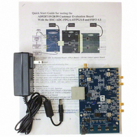
Page 37
... DEFAULT OPERATION AND JUMPER SELECTION SETTINGS The following is a list of the default and optional settings or modes allowed on the AD9219 Rev. A evaluation board. • POWER: Connect the switching power supply that is provided in the evaluation kit between a rated 100 240 V ac wall outlet and P503. ...
Page 38
... AD9219 ALTERNATIVE ANALOG INPUT DRIVE CONFIGURATION The following is a brief description of the alternative analog input drive configuration using the AD8332 dual VGA. If this drive option is in use, some components may need to be populated, in which case all the necessary components are listed in Table 17. For more details on the AD8332 dual VGA, including how it works and its optional pin settings, consult the AD8332 data sheet ...
Page 39
... C123 DNP 0Ω DNP 0.1µF CH_D FB112 CM4 10Ω E104 C127 R149 DNP C128 R150 1kΩ 0.1µF 1kΩ Rev Page AD9219 AVDD_DUT R152 DNP R108 33Ω VIN_A R109 C103 C104 1kΩ DNP 2.2pF VIN_A R110 C105 R156 33Ω DNP ...
Page 40
... AD9219 AVDD_DUT CW V– VIN_B 37 VIN_B 38 AVDD_DUT 39 40 VSENSE_DUT 41 VREF_DUT AVDD_DUT 45 AVDD_DUT 46 VIN_C 47 VIN_C 48 Figure 74. Evaluation Board Schematic, DUT, VREF, Clock Inputs, and Digital Output Interface 10kΩ R205 DNP - 100kΩ 100kΩ R267 R204 DNP - 100kΩ 100kΩ ...
Page 41
... LOP2 9 C314 0.1µF R317 C321 274Ω C325 C326 0.1µF 0.1µF 10µF C322 0.018µF C323 22pF L310 120nH C324 0.1µF INH3 AD9219 VG VG GND CW R319 10kΩ R314 10kΩ DNP R318 10kΩ ...
Page 42
... AD9219 FILTER. YOUR DESIGN OR RESISTORS 0Ω WITH L401-L408 POPULATE CH_A CH_A CH_B CH_B POWER) DISABLE = (0–1V ENABLE DOWN POWER Figure 76. Evaluation Board Schematic, Optional DUT Analog Input Drive and SPI Interface Circuit (Continued) SDO_CHA 0Ω R427 SDI_CHA 0Ω R420 SCLK_CHA 0Ω ...
Page 43
... Figure 77. Evaluation Board Schematic, Power Supply Inputs Rev Page AD9219 05726-019 GND GND 1 1 GND GND 1 1 ...
Page 44
... AD9219 Figure 78. Evaluation Board Layout, Primary Side Rev Page ...
Page 45
... Figure 79. Evaluation Board Layout, Ground Plane Rev Page AD9219 ...
Page 46
... AD9219 Figure 80. Evaluation Board Layout, Power Plane Rev Page ...
Page 47
... Figure 81. Evaluation Board Layout, Secondary Side (Mirrored Image) Rev Page AD9219 ...
Page 48
... AD9219 Table 17. Evaluation Board Bill of Materials (BOM) Item Qty. Reference Designator 1 1 AD9219LFCSP_REVA 2 75 C101, C102, C107, C108, C109, C114, C115, C116, C121, C122, C123, C128, C201, C203, C204, C205, C206, C210, C211, C212, C213, C216, C217, C218, C219, C220, C221, C222, ...
Page 49
... Resistor 402 64.9 Ω, 1/ tol Resistor 603 0 Ω, 1/ tol Resistor 402 1 kΩ, 1/ tol Resistor 402 33 Ω, 1/ tol Rev Page AD9219 Manufacturer’s Manufacturer Part Number Murata BLM18BA100SN1B Samtec TSW-102-07-G-S Samtec TSW-103-07-G-S Samtec TSW-104-08-G-T Samtec TSW-105-08-G-D Murata BLM31PG500SN1L Murata LQG15HNR12J02B ...
Page 50
... AD9219 Item Qty. Reference Designator 37 4 R161, R162, R163, R164 38 3 R202, R203, R204 39 1 R222 40 1 R213 41 1 R229 42 2 R230, R319 43 1 R228 44 1 R320 45 8 R307, R308, R309, R310, R407, R408, R409, R410 46 4 R305, R306, R405, R406 ...
Page 51
... NC7WZ16 MAA06A IC 8-SOIC Flash prog mem 1k × 14, RAM size 64 × MHz speed, PIC12F controller series Rev Page AD9219 Manufacturer’s Manufacturer Part Number Analog Devices ADP3339AKCZ-3.3 Analog Devices AD9219BCPZ-65 Analog Devices ADR510ARTZ Analog Devices AD9515BCPZ Fairchild NC7WZ07P6X_NL Fairchild NC7WZ16P6X_NL Microchip PIC12F629-I/SN ...
Page 52
... AD9219ABCPZRL7-40 −40°C to +85°C AD9219ABCPZ-65 −40°C to +85°C AD9219ABCPZRL7-65 −40°C to +85°C AD9219-65EBZ RoHS Compliant Part. ©2006–2010 Analog Devices, Inc. All rights reserved. Trademarks and registered trademarks are the property of their respective owners. 7.10 0.60 MAX 7 ...