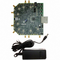
AD9212-65EBZ Analog Devices Inc, AD9212-65EBZ Datasheet - Page 28

AD9212-65EBZ
Manufacturer Part Number
AD9212-65EBZ
Description
Octal 10 Bit, 65 MSPS Serial LVDS ADC EB
Manufacturer
Analog Devices Inc
Datasheet
1.AD9212ABCPZRL7-40.pdf
(56 pages)
Specifications of AD9212-65EBZ
Number Of Adc's
8
Number Of Bits
10
Sampling Rate (per Second)
65M
Data Interface
Serial
Inputs Per Adc
1 Differential
Input Range
2 Vpp
Power (typ) @ Conditions
100mW @ 65MSPS
Voltage Supply Source
Analog and Digital
Operating Temperature
-40°C ~ 85°C
Utilized Ic / Part
AD9212
Lead Free Status / RoHS Status
Lead free / RoHS Compliant
AD9212
CSB Pin
The CSB pin should be tied to AVDD for applications that do
not require SPI mode operation. By tying CSB high, all SCLK
and SDIO information is ignored. This pin is both 1.8 V and
3.3 V tolerant.
RBIAS Pin
To set the internal core bias current of the ADC, place a resistor
that is nominally equal to 10.0 kΩ between the RBIAS pin and
ground. The resistor current is derived on chip and sets the
AVDD current of the ADC to a nominal 390 mA at 65 MSPS.
Therefore, it is imperative that at least a 1% tolerance on this
resistor be used to achieve consistent performance.
Voltage Reference
A stable, accurate 0.5 V voltage reference is built into the
AD9212. This is gained up internally by a factor of 2, setting
VREF to 1.0 V, which results in a full-scale differential input
span of 2 V p-p. VREF is set internally by default; however, the
VREF pin can be driven externally with a 1.0 V reference to
improve accuracy.
When applying the decoupling capacitors to the VREF, REFT,
and REFB pins, use ceramic low-ESR capacitors. These capacitors
should be close to the ADC pins and on the same layer of the
PCB as the AD9212. The recommended capacitor values and
configurations for the AD9212 reference pin are shown in
Figure 63.
Table 13. Reference Settings
Selected
Mode
External
Internal,
Internal Reference Operation
A comparator within the AD9212 detects the potential at the
SENSE pin and configures the reference. If SENSE is grounded,
the reference amplifier switch is connected to the internal
resistor divider (see Figure 63), setting VREF to 1 V.
The REFT and REFB pins establish their input span of the ADC
core from the reference configuration. The analog input full-
scale range of the ADC equals twice the voltage at the reference
pin for either an internal or an external reference configuration.
If the reference of the AD9212 is used to drive multiple
converters to improve gain matching, the loading of the refer-
ence by the other converters must be considered. Figure 65
depicts how the internal reference voltage is affected by loading.
Reference
2 V p-p FSR
SENSE
Voltage
AVDD
AGND to 0.2 V
Resulting
VREF (V)
N/A
1.0
Resulting
Differential
Span (V p-p)
2 × external
reference
2.0
Rev. D | Page 28 of 56
1µF
1
1µF
OPTIONAL.
REFERENCE
1
EXTERNAL
–10
–15
–20
–25
–30
SENSE
–5
0.1µF
SENSE
VIN + x
VIN – x
5
0
0.1µF
VIN + x
VIN – x
VREF
0
VREF
AVDD
1
Figure 63. Internal Reference Configuration
Figure 64. External Reference Operation
0.5
Figure 65. VREF Accuracy vs. Load
SELECT
LOGIC
SELECT
1.0
LOGIC
CURRENT LOAD (mA)
1.5
CORE
CORE
ADC
ADC
2.0
0.5V
0.5V
2.5
REFT
REFB
REFT
REFB
0.1µF
0.1µF
0.1µF
0.1µF
0.1µF
0.1µF
3.0
+
+
3.5
4.7µF
4.7µF


