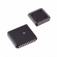
AD8600APZ Analog Devices Inc, AD8600APZ Datasheet - Page 8

AD8600APZ
Manufacturer Part Number
AD8600APZ
Description
16 CHANNEL 8-BIT MULT.DAC
Manufacturer
Analog Devices Inc
Datasheet
1.AD8600APZ-REEL.pdf
(16 pages)
Specifications of AD8600APZ
Rohs Compliant
YES
Settling Time
1µs
Number Of Bits
8
Data Interface
Parallel
Number Of Converters
16
Voltage Supply Source
Analog and Digital, Dual ±
Power Dissipation (max)
175mW
Operating Temperature
-40°C ~ 85°C
Mounting Type
Surface Mount
Package / Case
44-PLCC
Lead Free Status / RoHS Status
Lead free / RoHS Compliant
Available stocks
Company
Part Number
Manufacturer
Quantity
Price
Company:
Part Number:
AD8600APZ
Manufacturer:
Analog Devices Inc
Quantity:
10 000
Part Number:
AD8600APZ
Manufacturer:
ADI/亚德诺
Quantity:
20 000
Company:
Part Number:
AD8600APZ-REEL
Manufacturer:
Analog Devices Inc
Quantity:
10 000
AD8600
Operation
The AD8600 is a 16-channel voltage output, 8-bit digital to
analog converter. The AD8600 operates from a single +5 V
supply, or for a wider output swing range, the part can operate
from dual supplies of 5 V or 6 V or a single supply of +7 V.
The DACs are based upon a unique R-2R ladder structure*
that removes the possibility of current injection from the refer-
ence to ground during code switching. Each of the 8-bit DACs
has an output amplifier to provide 16 low impedance outputs.
With a single external reference, 16 independent dc output lev-
els can be programmed through a parallel digital interface. The
interface includes 4 bits of address (A0–A3), 8 bits of data
(DB0–DB7), a read/write select pin (R/W), an enable clock
strobe (EN), a DAC register load strobe (LD), and a chip select
pin (CS). Additionally a reset pin (RS) is provided to asynchro-
nously reset all 16 DACs to 0 V output.
D/A Converter Section
The internal DAC is an 8-bit voltage mode device with an out-
put that swings from DACGND to the external reference volt-
age, V
shown in Figure 16. The DAC uses an R-2R ladder to ensure
accuracy and linearity over the full temperature range of the part.
The switches shown are actually N and P-channel MOSFETs to
allow maximum flexibility and range in the choice of reference
voltage. The switches’ low ON resistance and matching is im-
portant in maintaining the accuracy of the R-2R ladder.
*Patent Pending.
DACGND
Figure 16. Equivalent Schematic of Analog Channel
V
REF
REF
Figure 14. Supply Current vs. Temperature
. The equivalent schematic of one of the DACs is
TO 15
DACs
20
19
18
17
16
15
–75
–50
V
V
V
–25
CC
EE
REF
TEMPERATURE – C
= –5V
= +5V
= 3.5V
R
R
R
R
0
25
R
R
R
R
50
R
R
2R
75
100
*R = 30k
TYPICALLY
R
125
V
OUT
–8–
Amplifier Section
The output of the DAC ladder is buffered by a rail-to-rail out-
put amplifier. This amplifier is configured as a unity gain fol-
lower as shown in Figure 16. The input stage of the amplifier
contains a PNP differential pair to provide low offset drift and
noise. The output stage is shown in Figure 17. It employs
complementary bipolar transistors with their collectors con-
nected to the output to provide rail-to-rail operation. The NPN
transistor enters into saturation as the output approaches the
negative rail. Thus, in single supply, the output low voltage is
limited by the saturation voltage of the transistor. For the tran-
sistors used in the AD8600, this is approximately 40 mV. The
AD8600 was not designed to swing to the positive rail in con-
trast to some of ADI’s other DACs (for example, the AD8582).
The output stage of the amplifier is actually capable of swinging
to the positive rail, but the input stage limits this swing to ap-
proximately 1.0 V below V
During normal operation, the output stage can typically source
and sink 1 mA of current. However, the actual short circuit
current is much higher. In fact, each DAC is capable of sourc-
ing 20 mA and sinking 8 mA during a short condition. The
absolute maximum ratings state that, at most, four DACs can
be shorted simultaneously. This restriction is due to current
densities in the metal traces. If the current density is too high,
voltage drops in the traces will cause a loss in linearity perfor-
mance for the other DACs in the package. Thus to ensure long-
term reliability, no more than four DACs should be shorted
simultaneously.
Figure 17. Equivalent Analog Output Circuit
–1
–2
–3
–4
–5
5
4
3
2
1
0
0
Figure 15. Output Voltage Drift
Accelerated by Burn-In
T = HOURS OF OPERATION AT +125 C
V
V
V
CODE = 00
200
CC
EE
REF
= –5V
= +5V
= 3.5V
CC
400
.
H
600
800
1000
1200
V
V
V
CC
OUT
EE
REV. 0


