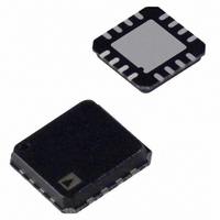
AD8398ACPZ-RL Analog Devices Inc, AD8398ACPZ-RL Datasheet - Page 8

AD8398ACPZ-RL
Manufacturer Part Number
AD8398ACPZ-RL
Description
Dual Wideband Hi Output Current OpAmp
Manufacturer
Analog Devices Inc
Type
Driverr
Datasheet
1.AD8398ACPZ-RL.pdf
(12 pages)
Specifications of AD8398ACPZ-RL
Number Of Drivers/receivers
2/0
Protocol
xDSL
Voltage - Supply
12V
Mounting Type
Surface Mount
Package / Case
16-LFCSP
Lead Free Status / RoHS Status
Lead free / RoHS Compliant
AD8398A
APPLICATIONS INFORMATION
POWER CONTROL MODES OF OPERATION
The AD8398A features four power modes: full power, medium
power, low power, and complete power-down. Two CMOS-
compatible logic pins (PD0 and PD1) select the power mode.
The power modes and associated logic states are listed in Table 5.
Table 5. Power Modes
PD1
0
0
1
1
EXPOSED THERMAL PAD CONNECTIONS
To ensure adequate heat transfer away from the die, connect
the exposed thermal pad to a solid plane layer with low thermal
resistance. To maximize the operating life of the AD8398A, the
thermal design of the system should be kept below the junction
temperature of 125°C.
Although it is electrically isolated, the thermal pad typically
connects to the ground plane layer.
POWER SUPPLY BYPASSING
The AD8398A typically operates on ±6 V or +12 V supplies.
Power the AD8398A circuit with a well-regulated, properly
decoupled power supply. To minimize supply voltage ripple
and power dissipation, use high quality capacitors with low
equivalent series resistance (ESR), such as multilayer ceramic
capacitors (MLCCs). Place a decoupling 0.1 μF MLCC no
more than ⅛ inch away from each of the power supply pins.
In addition, a 10 μF tantalum capacitor is recommended to
provide good decoupling for lower frequency signals and to
supply current for fast, large signal changes at the AD8398A
outputs. Lay out bypass capacitors to keep return currents away
from the inputs of the amplifiers. This layout minimizes any
voltage drops that can develop due to ground currents flowing
through the ground plane.
PD0
0
1
0
1
Power Mode
Full power
Medium power
Low power
Power-down
Total Supply Current (mA)
33.2
22.9
13.3
0.7
Rev. D | Page 8 of 12
BOARD LAYOUT
As is the case with all high speed applications, careful attention
to printed circuit board (PCB) layout details prevents associated
board parasitics from becoming problematic. Proper RF design
technique is mandatory.
The PCB has a ground plane covering all unused portions of the
component side of the board to provide a low impedance return
path. Removing the ground plane on all layers from the area
near the input and output pins of the AD8398A reduces stray
capacitance.
Signal lines connecting the feedback and gain resistors should
be as short as possible to minimize the inductance and stray
capacitance associated with these traces. Place termination resistors
and loads as close as possible to their respective inputs and outputs.
To minimize coupling (crosstalk) through the board, keep input
and output traces as far apart as possible. Wherever there are
complementary signals, provide a symmetrical layout to maximize
balanced performance.


