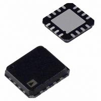
AD8398ACPZ-RL Analog Devices Inc, AD8398ACPZ-RL Datasheet - Page 4

AD8398ACPZ-RL
Manufacturer Part Number
AD8398ACPZ-RL
Description
Dual Wideband Hi Output Current OpAmp
Manufacturer
Analog Devices Inc
Type
Driverr
Datasheet
1.AD8398ACPZ-RL.pdf
(12 pages)
Specifications of AD8398ACPZ-RL
Number Of Drivers/receivers
2/0
Protocol
xDSL
Voltage - Supply
12V
Mounting Type
Surface Mount
Package / Case
16-LFCSP
Lead Free Status / RoHS Status
Lead free / RoHS Compliant
AD8398A
ABSOLUTE MAXIMUM RATINGS
Table 2.
Parameter
Power Supplies (V
Power Dissipation
Storage Temperature Range
Operating Temperature Range
Lead Temperature (Soldering, 10 sec)
Junction Temperature
Stresses above those listed under Absolute Maximum Ratings
may cause permanent damage to the device. This is a stress
rating only; functional operation of the device at these or any
other conditions above those indicated in the operational
section of this specification is not implied. Exposure to absolute
maximum rating conditions for extended periods may affect
device reliability.
THERMAL RESISTANCE
θ
board and the thermal pad connected to the GND plane layer
using six vias.
Table 3. Thermal Resistance
Package Type
16-Lead LFCSP_WQ
JA
is specified with the device soldered on a JEDEC circuit
CC
− V
EE
)
θ
35.6
JA
Rating
13.2 V
(T
−65°C to +125°C
−40°C to +85°C
300°C
150°C
J MAX
Unit
°C/W
− T
A
)/θ
JA
Rev. D | Page 4 of 12
MAXIMUM POWER DISSIPATION
The maximum safe power dissipation for the AD8398A is limited
by its junction temperature (T
T
transition temperature of the plastic, is 150°C. Temporarily
exceeding this limit may cause a shift in the parametric
performance due to a change in the stresses exerted on the
die by the package. Exceeding this limit for an extended period
can result in device failure.
Figure 3 shows the maximum safe power dissipation in the
package vs. the ambient temperature for the 16-lead LFCSP_WQ
on a 4-layer board with six vias connecting the exposed pad to
the GND plane layer.
ESD CAUTION
J
of plastic encapsulated devices, as determined by the glass
Figure 3. Maximum Safe Power Dissipation vs. Ambient Temperature,
6
5
4
3
2
1
0
–40 –30 –20 –10
4-Layer JEDEC Board with Six Thermal Vias
AMBIENT TEMPERATURE (°C)
0
10
J
) on the die. The maximum safe
20
30
40
50
60
T
J
70
= 150°C
80


