AD8330ARQ Analog Devices Inc, AD8330ARQ Datasheet - Page 3
AD8330ARQ
Manufacturer Part Number
AD8330ARQ
Description
QSOP SINGLE VGA
Manufacturer
Analog Devices Inc
Datasheet
1.AD8330-EVALZ.pdf
(32 pages)
Specifications of AD8330ARQ
Rohs Compliant
NO
Rohs Status
RoHS non-compliant
Amplifier Type
Variable Gain
Number Of Circuits
1
Output Type
Differential, Rail-to-Rail
Slew Rate
1500 V/µs
-3db Bandwidth
150MHz
Current - Input Bias
100nA
Current - Supply
20mA
Voltage - Supply, Single/dual (±)
2.7 V ~ 6 V
Operating Temperature
-40°C ~ 85°C
Mounting Type
Surface Mount
Package / Case
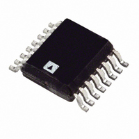
16-QSOP
For Use With
AD8330-EVALZ - BOARD EVAL FOR AD8330
Current - Output / Channel
-
Gain Bandwidth Product
-
Voltage - Input Offset
-
Lead Free Status / RoHS Status
Available stocks
Company
Part Number
Manufacturer
Quantity
Price

Part Number:
AD8330ARQ
Manufacturer:
ADI/亚德诺
Quantity:
20 000
Part Number:
AD8330ARQZ
Manufacturer:
ADI/亚德诺
Quantity:
20 000
Company:
Part Number:
AD8330ARQZ-REEL
Manufacturer:
JJM
Quantity:
1 200


SPECIFICATIONS
V
V
Table 1.
Parameter
INPUT INTERFACE
OUTPUT INTERFACE
OUTPUT OFFSET CONTROL
COMMON-MODE CONTROL
DECIBEL GAIN CONTROL
LINEAR GAIN INTERFACE
S
OFST
Full-Scale Input
Input Resistance
Input Capacitance
Voltage Noise Spectral Density
Common-Mode Voltage Level
Input Offset
Drift
Permissible CM Range
Common-Mode AC Rejection
Small Signal –3 dB Bandwidth
Peak Slew Rate
Peak-to-Peak Output Swing
Common-Mode Voltage
Voltage Noise Spectral Density
Differential Output Impedance
HD2
HD3
AC-Coupled Offset
High-Pass Corner Frequency
Usable Voltage Range
Input Resistance
Normal Voltage Range
Elevated Range
Gain Scaling
Gain Linearity Error
Absolute Gain Error
Bias Current
Incremental Resistance
Gain Settling Time to 0.5 dB Error
Mode Up/Down
Peak Output Scaling, Gain vs. V
Gain Multiplication Factor vs. V
Usable Input Range
Default Voltage
Incremental Resistance
Bandwidth
= 5 V, T
Mode Up Logic Level
Mode Down Logic Level
= 0 V, differential operation, unless otherwise noted.
2
2
A
= 25°C, C
L
= 12 pF on OPHI and OPLO, R
1
MAG
MAG
Pin OPHI, Pin OPLO
Conditions
Pin INHI, Pin INLO
V
V
Pin-to-pin
Either pin to COMM
f = 1 MHz, V
Pin OFST connected to Pin COMM
f = 1 MHz, 0.1 V rms
f = 50 MHz
0 V < V
V
V
Pin CNTR O/C
f = 1 MHz, V
Pin-to-pin
V
V
Pin OFST
C
C
Pin CNTR
From Pin CNTR to V
VDBS, CMGN, and MODE pins
CMGN connected to COMM
CMGN O/C (V
Mode high or low
0.3 V ≤ V
V
Flows out of Pin VDBS
V
Pin MODE
Gain increases with V
Gain decreases with V
Pin VMAG, Pin CMGN
See the Circuit Description section
Gain is nominal when V
V
For V
DBS
DBS
DBS
MAG
OUT
OUT
HPF
HPF
DBS
DBS
MAG
stepped from 0.05 V to 1.45 V or 1.45 V to 0.05 V
= 0 V, differential drive
= 1.5 V
= 0 V
on Pin OFST (0 V < V
= 3.3 nF, from OFST to CNTR (scales as 1/C
= 0 V
= 1 V p-p, f = 10 MHz, R
= 1 V p-p, f = 10 MHz, R
≥ 2 V (peaks are supply limited)
O/C
MAG
DBS
DBS
≥ 0.1 V
< 1.5 V
≤ 1.2 V
DBS
DBS
L
CMGN
= ∞, V
= 1.5 V; inputs ac-shorted
= 0 V
rises to 0.2 V)
Rev. E | Page 3 of 32
S
/2
DBS
DBS
DBS
MAG
, MODE = O/C
= 0.75 V, V
DBS
= 0.5 V
< 1.5 V)
L
L
= 1 kΩ
= 1 kΩ
MODE
= high, V
HPF
)
MAG
= Pin VMAG open circuit (0.5 V),
Min
±1.4
±4.5
800
0
±1.8
±4
2.4
120
0.5
27
−0.35
−2
1.5
3.8
0
0.48
Typ
±2
±6.3
1 k
4
5
3.0
1
2
−60
−55
150
1500
±2
±4.5
2.5
62
150
−62
−53
10
100
4
0 to 1.5
0.2 to 1.7
30
±0.1
±0.5
100
100
250
4.0
×2
0.5
4
150
Max
1.2 k
V
±2.2
2.6
180
4.5
33
+0.35
+2
0.5
4.2
5
0.52
S
AD8330
Unit
V
mV
pF
nV/√Hz
V
mV rms
μV/°C
V
dB
dB
MHz
V/μs
V
nV/√Hz
Ω
dBc
dBc
mV rms
kHz
V
kΩ
dB
dB
nA
MΩ
V
V
V/V
V
V
kΩ
MHz
Ω
V
V
V
V
mV/dB
ns
Related parts for AD8330ARQ
Image
Part Number
Description
Manufacturer
Datasheet
Request
R

Part Number:
Description:
BOARD EVAL FOR AD8330
Manufacturer:
Analog Devices Inc
Datasheet:

Part Number:
Description:
BOARD EVAL FOR AD8330
Manufacturer:
Analog Devices Inc
Datasheet:

Part Number:
Description:
±1.7g Dual-Axis IMEMS Accelerometer Evaluation Board
Manufacturer:
Analog Devices Inc
Datasheet:

Part Number:
Description:
Inertial Sensor Evaluation System
Manufacturer:
Analog Devices Inc
Datasheet:
Part Number:
Description:
Manufacturer:
Analog Devices Inc
Datasheet:
Part Number:
Description:
Manufacturer:
Analog Devices Inc
Datasheet:
Part Number:
Description:
Manufacturer:
Analog Devices Inc
Datasheet:
Part Number:
Description:
Manufacturer:
Analog Devices Inc
Datasheet:
Part Number:
Description:
Manufacturer:
Analog Devices Inc
Datasheet:
Part Number:
Description:
Manufacturer:
Analog Devices Inc
Datasheet:
Part Number:
Description:
Manufacturer:
Analog Devices Inc
Datasheet:
Part Number:
Description:
Manufacturer:
Analog Devices Inc
Datasheet:
Part Number:
Description:
Manufacturer:
Analog Devices Inc
Datasheet: