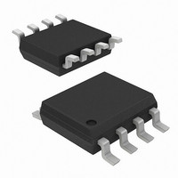
AD8314ARM Analog Devices Inc, AD8314ARM Datasheet - Page 19

AD8314ARM
Manufacturer Part Number
AD8314ARM
Description
Amplifier IC Bandwidth:2500MHz
Manufacturer
Analog Devices Inc
Datasheet
1.AD8314ACPZ-RL7.pdf
(20 pages)
Specifications of AD8314ARM
Amplifier Type
RoHS Compliant
Rohs Status
RoHS non-compliant
Frequency
100MHz ~ 2.7GHz
Rf Type
Cellular, GSM, TDMA, CDMA
Input Range
-45dBm ~ 0dBm
Voltage - Supply
2.7 V ~ 5.5 V
Current - Supply
5.7mA
Package / Case
8-TSSOP, 8-MSOP (0.118", 3.00mm Width)
Accuracy
-
Lead Free Status / RoHS Status
Available stocks
Company
Part Number
Manufacturer
Quantity
Price
Company:
Part Number:
AD8314ARM
Manufacturer:
AD
Quantity:
5 321
Part Number:
AD8314ARM
Manufacturer:
AD
Quantity:
20 000
Company:
Part Number:
AD8314ARM-REEL7
Manufacturer:
AD
Quantity:
5 379
Part Number:
AD8314ARM-REEL7
Manufacturer:
ADI/亚德诺
Quantity:
20 000
Company:
Part Number:
AD8314ARMZ
Manufacturer:
AD
Quantity:
5 510
Part Number:
AD8314ARMZ
Manufacturer:
ADI/亚德诺
Quantity:
20 000
Part Number:
AD8314ARMZ-REEL7
Manufacturer:
ADI/亚德诺
Quantity:
20 000
Table 7. Evaluation Board Configuration Options
Component
TP1, TP2
SW1
R1, R2
R3, R4, C2,
R5, R6, C3
C1, R9
C4
R7, R8
LK1
Figure 46. Layout of Component Side (MSOP)
Function
Supply and Ground Vector Pins.
Device Enable: When in Position A, the ENBL pin is connected to +V
operating mode. In Position B, the ENBL pin is grounded, putting the device in power-down mode.
Input Interface. The 52.3 Ω resistor in Position R2 combines with the AD8314’s internal input
impedance to give a broadband input impedance of around 50 Ω. A reactive match can be
implemented by replacing R2 with an inductor and R1 (0 Ω) with a capacitor. Note that the
AD8314’s RF input is internally ac-coupled.
Output Interface. R4, C2, R6, and C3 can be used to check the response of V_UP and V_DN to
capacitive and resistive loading. R3/R4 and R5/R6 can be used to reduce the slope of V_UP
and V_DN.
Power Supply Decoupling. The nominal supply decoupling consists of a 0.1 μF capacitor (C1).
A series inductor or small resistor can be placed in R9 for additional decoupling.
Filter Capacitor. The response time of V_UP and V_DN can be modified by placing a capacitor
between FILTR and V_UP.
Slope Adjust. By installing resistors in R7 and R8, the nominal slope of 20 mV/dB can be
increased. See Increasing the Logarithmic Slope in Measurement Mode for more details.
Measurement/Controller Mode. LK1 shorts V_UP to VSET, placing the AD8314 in measurement
mode. Removing LK1 places the AD8314 in controller mode.
Rev. B | Page 19 of 20
S
and the AD8314 is in
Figure 47. Silkscreen of Component Side (MSOP)
Default Condition
Not Applicable
SW1 = A
R2 = 52.3 Ω (Size 0603)
R1 = 0 Ω (Size 0402)
R4 = C2 = R6 =
C3 = Open (Size 0603)
R3= R5 = 0 Ω (Size 0603)
C1 = 0.1 μF (Size 0603)
R9 = 0 Ω (Size 0603)
C4 = Open (Size 0603)
R7 = 0 Ω (Size 0603)
R8 = Open (Size 0603)
LK1 = Installed
AD8314


