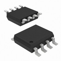
AD8314ARM Analog Devices Inc, AD8314ARM Datasheet - Page 17

AD8314ARM
Manufacturer Part Number
AD8314ARM
Description
Amplifier IC Bandwidth:2500MHz
Manufacturer
Analog Devices Inc
Datasheet
1.AD8314ACPZ-RL7.pdf
(20 pages)
Specifications of AD8314ARM
Amplifier Type
RoHS Compliant
Rohs Status
RoHS non-compliant
Frequency
100MHz ~ 2.7GHz
Rf Type
Cellular, GSM, TDMA, CDMA
Input Range
-45dBm ~ 0dBm
Voltage - Supply
2.7 V ~ 5.5 V
Current - Supply
5.7mA
Package / Case
8-TSSOP, 8-MSOP (0.118", 3.00mm Width)
Accuracy
-
Lead Free Status / RoHS Status
Available stocks
Company
Part Number
Manufacturer
Quantity
Price
Company:
Part Number:
AD8314ARM
Manufacturer:
AD
Quantity:
5 321
Part Number:
AD8314ARM
Manufacturer:
AD
Quantity:
20 000
Company:
Part Number:
AD8314ARM-REEL7
Manufacturer:
AD
Quantity:
5 379
Part Number:
AD8314ARM-REEL7
Manufacturer:
ADI/亚德诺
Quantity:
20 000
Company:
Part Number:
AD8314ARMZ
Manufacturer:
AD
Quantity:
5 510
Part Number:
AD8314ARMZ
Manufacturer:
ADI/亚德诺
Quantity:
20 000
Part Number:
AD8314ARMZ-REEL7
Manufacturer:
ADI/亚德诺
Quantity:
20 000
Figure 40 shows the relationship between the setpoint voltage,
V
function is linear in dB for a dynamic range of over 40 dB.
Figure 41 shows a similar circuit for a single band handset
power amplifier. The BGY241 (Phillips) is driven by a nominal
power level of 0 dBm. A 20 dB directional coupler, DC09-73
(Alpha), is used to couple the signal in this case. Figure 42
shows the relationship between the control voltage and the
output power at 0.9 GHz.
In both of these examples, noise on the V_DN pin can be reduced
by placing a simple RC low-pass filter between V
control pin of the power amplifier. However, the value of the
resistor should be kept low to minimize the voltage drop across
it due to the dc current flowing into the gain control input.
Figure 40. POUT vs. VSET at 0.9 GHz for Dual Mode Handset Power Amplifier
SET
and output power at 0.9 GHz. The overall gain control
–10
–20
–30
40
30
20
10
0
0
0.2
0.4
Application
VSET (V)
0.6
0.8
1.0
DN
and the gain
1.2
Rev. B | Page 17 of 20
0V TO 1.1V
ANTENNA
ATTN
15dB
TO
VSET
Figure 42. POUT vs. VSET at 0.9 GHz for Single Mode Handset
–10
–20
–30
–40
–50
40
30
20
10
Figure 41. A Single Mode Power Amplifier Control Circuit
0
0
15dBm
0dBm
MAX
52.3Ω
V
S
6
3
DC09-73
0.2
1
1
2
3
4
RFIN
ENBL
VSET
FLTR
2
4
5
AD8314
0.4
35dBm
220pF
MAX
C
F
VSET (V)
COMM
VPOS
V_DN
V_UP
0.6
BGY241
8
7
6
5
0.1µF
680pF
2.2µF
3.5V
47µF
0.8
RF INPUT
V
2.7V
S
AD8314
1.0
P
0dBm
IN


