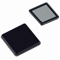
AD8190ACPZ Analog Devices Inc, AD8190ACPZ Datasheet - Page 18

AD8190ACPZ
Manufacturer Part Number
AD8190ACPZ
Description
IC,Telecom Switching Circuit,LLCC,56PIN,PLASTIC
Manufacturer
Analog Devices Inc
Datasheet
1.AD8190ACPZ-R7.pdf
(24 pages)
Specifications of AD8190ACPZ
Applications
*
Mounting Type
Surface Mount
Package / Case
56-LFCSP
Lead Free Status / RoHS Status
Lead free / RoHS Compliant
For Use With
AD8190-9880/PCB - KIT EVAL FOR AD8190 & AD9880
Lead Free Status / RoHS Status
Lead free / RoHS Compliant
Available stocks
Company
Part Number
Manufacturer
Quantity
Price
Company:
Part Number:
AD8190ACPZ
Manufacturer:
ADI
Quantity:
329
Part Number:
AD8190ACPZ
Manufacturer:
ADI/亚德诺
Quantity:
20 000
Part Number:
AD8190ACPZ-R7
Manufacturer:
ADI/亚德诺
Quantity:
20 000
AD8190
APPLICATION NOTES
The AD8190 is an HDMI/DVI switch featuring equalized
TMDS inputs and pre-emphasized TMDS outputs. It is in-
tended for use as a 2:1 switch in systems with long cable runs
on both the input and/or the output, and is fully HDMI 1.2a
receive compliant.
PINOUT
The AD8190 was designed to have an HDMI/DVI receiver
pinout at its input and a transmitter pinout at its output. This
makes the AD8190 ideal for use in AVR-type applications
where a designer routes both the inputs and the outputs directly
to HDMI/DVI connectors as shown in Figure 31. When the
AD8190 is used in receiver-type applications, it is necessary to
change the ordering of the output pins on the PCB to match up
with the on-board receiver, as shown in Figure 32.
One advantage of the AD8190 in an AVR-type application is
that all of the high speed signals can be routed on one side (the
topside) of the board, as shown in Figure 31. In addition to
12 dB of input equalization, the AD8190 provides up to 6 dB of
output pre-emphasis that boosts the output TMDS signals and
allows the AD8190 to precompensate when driving long PCB
traces or output cables. The net effect of the input equalization
and output pre-emphasis of the AD8190 is that the AD8190 can
compensate for the signal degradation of both input and output
cables; it acts to reopen a closed input data eye and transmit a
full-swing HDMI signal to an end receiver. More information
on the specific performance metrics of the AD8190 can be
found in the Typical Performance Characteristics section.
The AD8190 also provides a distinct advantage in receive-type
applications because it is a fully buffered HDMI/DVI switch.
Figure 31. Evaluation Board Layout of the TMDS Traces
Rev. 0 | Page 18 of 24
Although inverting the output pin order of the AD8190 on the
PCB requires a designer to place vias in the high speed signal
path, the AD8190 fully buffers and electrically decouples the
outputs from the inputs. Therefore, the effects of the vias placed
on the output signal lines are not seen at the input of the AD8190.
The programmable output terminations also improve signal
quality at the output of the AD8190. The PCB designer, there-
fore, has significantly improved flexibility in the placement and
routing of the output signal path with the AD8190 over other
solutions.
An example of high speed routing from an HDMI Standard
Revision 1.2a receive-compliant reference design is shown in
Figure 32. The light gray TMDS lines are routed on the top layer
of the PCB, the dark gray TMDS lines are routed on the bottom
layer, and the black dots are vias.
Figure 32. Layout of the TMDS Traces for the AD8190 in an HDMI Standard
HDMI IN
HDMI IN
J4
Revision 1.2a Receive-Compliant Reference Design
AD8190
AD9880 (Rx)


