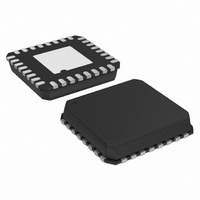
AD8153ACPZ-RL7 Analog Devices Inc, AD8153ACPZ-RL7 Datasheet

AD8153ACPZ-RL7
Specifications of AD8153ACPZ-RL7
Available stocks
Related parts for AD8153ACPZ-RL7
AD8153ACPZ-RL7 Summary of contents
Page 1
FEATURES Single lane 2:1 mux/1:2 demux 3.2 Gbps to dc data rates Compensates over 40 inches of FR4 at 3.2 Gbps through Two levels of input equalization, or Four levels of output pre-emphasis Operates with ac- or dc-coupled differential I/O ...
Page 2
AD8153 TABLE OF CONTENTS Features .............................................................................................. 1 Applications....................................................................................... 1 Functional Block Diagram .............................................................. 1 General Description ......................................................................... 1 Revision History ............................................................................... 2 Specifications..................................................................................... Timing Specifications............................................................ 4 Absolute Maximum Ratings............................................................ 5 ESD Caution.................................................................................. 5 Pin Configuration and ...
Page 3
SPECIFICATIONS 3 TTI TTO EE L pattern 800 mV p- 25°C, unless otherwise noted Table 1. Parameter Conditions DYNAMIC PERFORMANCE Data ...
Page 4
AD8153 TIMING SPECIFICATIONS SDA LOW SCL t HD;STA t HD;DAT S Table 2. Parameter SCL Clock Frequency Hold Time for a Start Condition Set-up Time for a Repeated Start Condition Low Period ...
Page 5
ABSOLUTE MAXIMUM RATINGS Table 3. Parameter Rating 3 0.6 V TTI 0.6 V TTO CC Internal Power Dissipation 4.1 W Differential Input Voltage 2.0 V Logic Input ...
Page 6
AD8153 PIN CONFIGURATION AND FUNCTION DESCRIPTIONS Table 4. Pin Function Descriptions Pin No. Mnemonic VCC 2 VTTO 3 ONA 4 OPA 5 VTTI 6 INA 7 IPA 8, 32, EPAD VEE 10 ONB 11 OPB 13 INB ...
Page 7
TYPICAL PERFORMANCE CHARACTERISTICS =3 Ω, two outputs active with no pre-emphasis, high EQ, data rate = 3.2 Gbps, ac-coupled, CC TTI TTO EE L PRBS7 test pattern, ...
Page 8
AD8153 DATA OUT PATTERN GENERATOR 40ps/DIV REFERENCE EYE DIAGRAM AT TP1 40ps/DIV Figure 8. 3.2 Gbps Input Eye, 20 Inch FR4 Input Channel (TP2 from Figure 7) 40ps/DIV Figure 9. 3.2 Gbps Input Eye, 40 Inch FR4 Input Channel (TP2 ...
Page 9
DATA OUT PATTERN GENERATOR 40ps/DIV REFERENCE EYE DIAGRAM AT TP1 40ps/DIV Figure 13. 3.2 Gbps Output Eye, Pre-Channel (TP2 from Figure 12) 40ps/DIV Figure 14. 3.2 Gbps Output Eye, Pre-Channel (TP2 from Figure 12) ...
Page 10
AD8153 LOW HIGH FR4 INPUT CHANNEL LENGTH (IN) Figure 17. Deterministic Jitter vs. FR4 Input Channel Length DETERMINISTIC JITTER 30 20 ...
Page 11
DETERMINISTIC JITTER 20 10 RANDOM JITTER 0 3.0 3.1 3.2 3.3 3.4 V (V) CC Figure 23. Jitter vs. Core Supply Voltage DETERMINISTIC JITTER 10 RANDOM JITTER ...
Page 12
AD8153 1000 900 800 700 600 500 400 300 200 100 0 3.0 3.1 3.2 3.3 V (V) CC Figure 29. Eye Height vs. Core Supply Voltage 3.4 3.5 3.6 Rev Page 1000 900 800 ...
Page 13
THEORY OF OPERATION The AD8153 consists of a 2:1 multiplexer and a 1:2 demultiplexer. There are three operating modes: pin mode, serial mode, and mixed mode. In pin mode, lane switching, equalization, and pre-emphasis are controlled using external pins. In ...
Page 14
AD8153 LB_A LB_B LB_C RECEIVE EQUALIZATION In backplane applications, the AD8153 needs to compensate for signal degradation caused by long traces. The device supports two ...
Page 15
I C SERIAL CONTROL INTERFACE REGISTER SET The AD8153 can be controlled in one of three modes: pin mode, serial mode, and mixed mode. In pin mode, the AD8153 control is derived from the package pins, whereas in serial ...
Page 16
AD8153 DATA WRITE To write data to the AD8153 register set, a microcontroller any other I C master, needs to send the appropriate control signals to the AD8153 slave device. The steps that need to ...
Page 17
I C DATA READ To read data from the AD8153 register set, a microcontroller any other I C master, needs to send the appropriate control signals to the AD8153 slave device. The steps to be followed are ...
Page 18
AD8153 APPLICATIONS INFORMATION The main application of the AD8153 is to support redundancy on both the backplane side and the line interface side of a serial link. Figure 34 illustrates redundancy in a typical backplane system. Each line card is ...
Page 19
PCB DESIGN GUIDELINES Proper RF PCB design techniques must be used for optimal performance. Power Supply Connections and Ground Planes Use of one low impedance ground plane is recommended. The VEE pins should be soldered directly to the ground plane ...
Page 20
AD8153 INTERFACING TO THE AD8153 TERMINATION STRUCTURES To determine the best strategy for connecting to the high speed pins of the AD8153, the user must first be familiar with the on- chip termination structures. The AD8153 contains two types of ...
Page 21
OUTPUT COMPLIANCE Figure graphical depiction of the single-ended waveform at the output of the AD8153. The common-mode level (V and the amplitude ( this waveform are a function of the OSE output tail current (I ...
Page 22
... THE PACKAGE AND ELECTRICALLY CONNECTED TO V TRACES OR VIAS BE LOCATED UNDER THE PACKAGE THAT COULD COME IN CONTACT WITH THE CONDUCTIVE SLUG. ORDERING GUIDE Model Temperature Range AD8153ACPZ 1 −40°C to +85°C 1 AD8153ACPZ-RL7 −40°C to +85°C AD8153-EVALZ RoHS Compliant Part. 5.00 BSC SQ 0.60 MAX 24 ...
Page 23
NOTES Rev Page AD8153 ...
Page 24
AD8153 NOTES ©2007 Analog Devices, Inc. All rights reserved. Trademarks and registered trademarks are the property of their respective owners. D06393-0-4/07(0) Rev Page ...


