AD8152JBPZ Analog Devices Inc, AD8152JBPZ Datasheet - Page 3
AD8152JBPZ
Manufacturer Part Number
AD8152JBPZ
Description
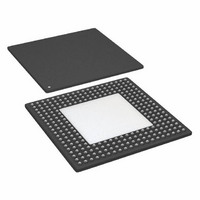
IC,Telecom Switching Circuit,BGA,256PIN,PLASTIC
Manufacturer
Analog Devices Inc
Datasheet
1.AD8152JBPZ.pdf
(32 pages)
Specifications of AD8152JBPZ
Function
Crosspoint Switch
Circuit
1 x 34:34
Voltage Supply Source
Single Supply
Voltage - Supply, Single/dual (±)
2.5 V ~ 3.3 V
Current - Supply
32mA
Operating Temperature
0°C ~ 85°C
Mounting Type
Surface Mount
Package / Case
256-BGA Exposed Pad, 256-eBGA, 256-HBGA
Lead Free Status / RoHS Status
Lead free / RoHS Compliant
Available stocks
Company
Part Number
Manufacturer
Quantity
Price
Company:

Part Number:
AD8152JBPZ
Manufacturer:
ADI
Quantity:
642
Company:
Part Number:
AD8152JBPZ
Manufacturer:
Analog Devices Inc
Quantity:
10 000


ABSOLUTE MAXIMUM RATINGS
VCC to VEE . . . . . . . . . . . . . . . . . . . . . . . . . . . . . . . . . . 3.7 V
VTTI . . . . . . . . . . . . . . . . . . . . . . . . . . . . . . . . . VCC + 0.6 V
VTTO . . . . . . . . . . . . . . . . . . . . . . . . . . . . . . . . . VCC + 0.6 V
Internal Power Dissipation
Input Voltage . . . . . . . . . . . . . . . . . . . . . . . . . . . . VCC + 0.6 V
Differential Input Voltage . . . . . . . . . . . . . . . . . . . . . . . . 1.7 V
Logic Input Voltage . . . . . . VEE – 0.3 V < V
Storage Temperature Range . . . . . . . . . . . . . –65°C to +125°C
Lead Temperature Range . . . . . . . . . . . . . . . . . . . . . . . 300°C
NOTES
1
2
MAXIMUM POWER DISSIPATION
The maximum power that can be safely dissipated by the AD8152 is
limited by the associated rise in junction temperature. The maxi-
mum safe junction temperature for plastic encapsulated devices
is determined by the glass transition temperature of the plastic,
approximately 150°C. Temporarily exceeding this limit may cause
CAUTION
ESD (electrostatic discharge) sensitive device. Electrostatic charges as high as 4000 V readily
accumulate on the human body and test equipment and can discharge without detection. Although the
AD8152 features proprietary ESD protection circuitry, permanent damage may occur on devices
subjected to high energy electrostatic discharges. Therefore, proper ESD precautions are recommended
to avoid performance degradation or loss of functionality.
REV. A
Stresses above those listed under Absolute Maximum Ratings may cause perma-
nent damage to the device. This is a stress rating only; functional operation of the
device at these or any other conditions above those indicated in the operational
sections of this specification is not implied. Exposure to absolute maximum rating
conditions for extended periods may affect device reliability.
Specification is for the device in free air (T
AD8152 256-Ball SBGA (BP) . . . . . . . . . . . . . . . . . . 8.33 W
Model
AD8152JBP
AD8152-EVAL
2
A
= 25°C):
1
Temperature Range
0°C to 85°C
JA
IN
= 15°C/W @ still air.
< VCC + 0.6 V
ORDERING GUIDE
–3–
a shift in parametric performance due to a change in the stresses
exerted on the die by the package. Exceeding a junction tem-
perature of 175°C for an extended period can result in device
failure. To ensure proper operation, it is necessary to observe the
maximum power derating curves shown in Figure 2.
Figure 2. Maximum Power Dissipation vs. Temperature
Package Description
256-Ball SBGA (27 mm × 27 mm)
Evaluation Board
16
14
12
10
8
6
4
2
0
0
10
20
200 lfpm
AMBIENT TEMPERATURE – C
STILL AIR
30
400 lfpm
40
50
60
70
AD8152
Tj = 150 C
80
90
Related parts for AD8152JBPZ
Image
Part Number
Description
Manufacturer
Datasheet
Request
R

Part Number:
Description:
SENSOR GAS FOR CO/NO2 EXHAUST
Manufacturer:
GE Sensing
Datasheet:

Part Number:
Description:
±1.7g Dual-Axis IMEMS Accelerometer Evaluation Board
Manufacturer:
Analog Devices Inc
Datasheet:

Part Number:
Description:
Inertial Sensor Evaluation System
Manufacturer:
Analog Devices Inc
Datasheet:
Part Number:
Description:
Manufacturer:
Analog Devices Inc
Datasheet:
Part Number:
Description:
Manufacturer:
Analog Devices Inc
Datasheet:
Part Number:
Description:
Manufacturer:
Analog Devices Inc
Datasheet:
Part Number:
Description:
Manufacturer:
Analog Devices Inc
Datasheet:
Part Number:
Description:
Manufacturer:
Analog Devices Inc
Datasheet:
Part Number:
Description:
Manufacturer:
Analog Devices Inc
Datasheet:
Part Number:
Description:
Manufacturer:
Analog Devices Inc
Datasheet:
Part Number:
Description:
Manufacturer:
Analog Devices Inc
Datasheet:
Part Number:
Description:
Manufacturer:
Analog Devices Inc
Datasheet:
Part Number:
Description:
Manufacturer:
Analog Devices Inc
Datasheet: