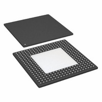
AD8152JBPZ Analog Devices Inc, AD8152JBPZ Datasheet - Page 21

AD8152JBPZ
Manufacturer Part Number
AD8152JBPZ
Description
IC,Telecom Switching Circuit,BGA,256PIN,PLASTIC
Manufacturer
Analog Devices Inc
Datasheet
1.AD8152JBPZ.pdf
(32 pages)
Specifications of AD8152JBPZ
Function
Crosspoint Switch
Circuit
1 x 34:34
Voltage Supply Source
Single Supply
Voltage - Supply, Single/dual (±)
2.5 V ~ 3.3 V
Current - Supply
32mA
Operating Temperature
0°C ~ 85°C
Mounting Type
Surface Mount
Package / Case
256-BGA Exposed Pad, 256-eBGA, 256-HBGA
Lead Free Status / RoHS Status
Lead free / RoHS Compliant
Available stocks
Company
Part Number
Manufacturer
Quantity
Price
Company:
Part Number:
AD8152JBPZ
Manufacturer:
ADI
Quantity:
642
Company:
Part Number:
AD8152JBPZ
Manufacturer:
Analog Devices Inc
Quantity:
10 000
First, the output current can be programmed to the smallest amount
required to maintain BER performance. If an output circuit
always has a short length and the receiver has good sensitivity,
then a lower output current can be used.
It is also possible to lower the voltage on VTTO to lower the
power dissipation. The amount that VTTO can be lowered is
dependent on the lowest of all the output’s V
determined by the output that is operating at the highest pro-
grammed output current since V
EVALUATION BOARD AND PCB LAYOUT HINTS
The AD8152 evaluation board was designed to allow the user to
analyze signal integrity in many configurations, as controlled by
a standard PC.
The FR4 board comes equipped with a full complement of
136 SMA connectors to support the complete 34
points. Each differential pair of microstrip is connected to either
top mount or side-launch SMA connectors. The mounting area of
the short center pin top-mount SMA connectors are drilled (seven
holes) and stubbed for greatly improved performance. In the
area surrounding SMA top-mount center pin and drill holes, all
internal planes are relieved or cleared out (see Figure 10 for layout).
REV. A
DIELECTRIC
THICKNESS
16.0mils
16.0mils
0.5mils
5.0mils
4.0mils
4.0mils
4.0mils
5.0mils
0.5mils
OL
= VTTO – (I
SILKSCREEN
SILKSCREEN
OL
Figure 11. Evaluation Board Stack-Up
. This will be
OUT
34 matrix of
¥ 25 W).
–21–
COPPER
LAYER
NUMBER
1.
2.
3.
4.
5.
6.
7.
8.
The FR4 PC board is eight layers with a thickness of 62 mils
(1.57 mm). The two outer most metal layers hold the high speed
microstrip routing lines. The two outer most dielectric layers are
5 mils thick and must be controlled impedance (50 W) layers. These
are the only two layers that require controlled impedance. The
next two inner metal layers are ground (reference) planes for the
microstrip and are the shell for the SMA connectors. The remain-
ing four inner metal layers are for the four AD8152 supply and
digital control signal routing. From top to bottom the four supply
layers are VTTO, VCC, VEE, and VTTI. Because all four supply
PCB metal layers float, positive, negative, and even dual-supply
configurations are possible. The variety of supply configurations
ease the connection of test equipment. The four inner supply
layers also provide an interlayer capacitance, which has better
impedance versus frequency than standard chip capacitors.
MICROSTRIP
TOP VIEW OF TOP LEVEL TRACE
Figure 10. Top-Mount SMA PCB Layout, Two Views
SMA CENTER PIN
THICKNESS/DESIGNATION
(IN OUNCES)
1.50/ TOP MICROSTRIP WIDTH = 8.0mils
0.50/GND
0.50/VTTO
0.50/VCC
0.50/VEE
0.50/VTTI
0.50/GND
1.50/BOTTOM MICROSTRIP WIDTH = 8.0mils
ALL TOP-MOUNT SMAs SIT ON PCB TOP LEVEL
DRILL HOLES
(7 EACH)
PLANE RELIEF
BOTTOM VIEW OF BOTTOM LEVEL TRACE
AD8152


