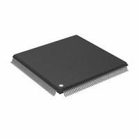
AD8150ASTZ Analog Devices Inc, AD8150ASTZ Datasheet - Page 14

AD8150ASTZ
Manufacturer Part Number
AD8150ASTZ
Description
IC,Telecom Switching Circuit,QFP,184PIN,PLASTIC
Manufacturer
Analog Devices Inc
Datasheet
1.AD8150AST.pdf
(44 pages)
Specifications of AD8150ASTZ
Function
Crosspoint Switch
Circuit
1 x 33:17
Voltage Supply Source
Dual Supply
Voltage - Supply, Single/dual (±)
±3 V ~ 5.5 V
Operating Temperature
0°C ~ 85°C
Mounting Type
Surface Mount
Package / Case
184-LQFP
Lead Free Status / RoHS Status
Lead free / RoHS Compliant
Available stocks
Company
Part Number
Manufacturer
Quantity
Price
Company:
Part Number:
AD8150ASTZ
Manufacturer:
Analog Devices Inc
Quantity:
10 000
AD8150
CONTROL INTERFACE
CONTROL INTERFACE TRUTH TABLES
The following are truth tables for the control interface.
Table 4. Basic Control Functions
RESET
0
1
1
1
1
1
Table 5. Address Data Examples
A4
0
1
<Binary Output Number
<Binary Output Number
1
1
1
The binary output number may also be the broadcast connection designator, 10001X.
Output Address Pins
A3
0
0
0
0
MSB to LSB
CS
X
1
0
0
0
0
Control Pins
A2
0
0
0
0
WE
X
X
0
X
X
0
A1
0
0
0
1
RE
X
X
X
0
X
1
A0
0
0
1
0
1
1
>
>
UPDATE
X
X
X
X
0
0
Enable
Bit
D6/E
X
X
1
0
X
X
Function
Global Reset. Reset all second-rank enable bits to 0 (disable all outputs).
Control Disable. Ignore all logic (but the signal matrix still functions as programmed). D[6:0] are high
impedance.
Single Output Preprogram. Write input configuration data from Data Bus D[6:0] into first rank of
latches for the output selected by the Output Address Bus A[4:0].
Single Output Readback. Readback input configuration data from second rank of latches onto Data
Bus D[6:0] for the single output selected by the Output Address Bus A[4:0].
Global Update. Copy input configuration data from all 17 first-rank latches into second rank of
latches, updating signal matrix connections for all outputs.
Transparent Write and Update. It is possible to write data directly onto rank two. This simplifies logic
when synchronous signal matrix updating is not necessary.
D5
0
1
<Binary Input Number>
X
<Binary Input Number>
1
D4
0
0
X
0
Input Address Pins
MSB to LSB
D3
0
0
X
0
D2
0
0
X
0
Rev. A | Page 14 of 44
D1
0
0
X
0
D0
0
0
X
1
Lower Address/Data Range. Connect Output 00
(A[4:0] = 00000) to Input 00 (D[5:0] = 000000).
Upper Address/Data Range. Connect Output 16
(A[4:0] = 10000) to Input 32 (D[5:0] = 100000).
Enable Output. Connect selected output (A[4:0] = 0 to 16) to
designated input (D[5:0] = 0 to 32) and enable output
(D6 = 1).
Disable Output. Disable specified output (D6 = 0).
Broadcast Connection. Connect all 17 outputs to the same
designated input and set all 17 enable bits to the value of
D6. Readback is not possible with the broadcast address.
Reserved. Any address or data code greater or equal to these
are reserved for future expansion or factory testing.
Function


