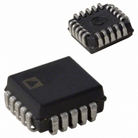
AD7821KPZ Analog Devices Inc, AD7821KPZ Datasheet - Page 4

AD7821KPZ
Manufacturer Part Number
AD7821KPZ
Description
8-BIT ATC CONVERTER IC
Manufacturer
Analog Devices Inc
Datasheet
1.AD7821KRZ-REEL.pdf
(16 pages)
Specifications of AD7821KPZ
Number Of Bits
8
Sampling Rate (per Second)
1M
Data Interface
Parallel
Number Of Converters
3
Power Dissipation (max)
50mW
Voltage Supply Source
Dual ±
Operating Temperature
-40°C ~ 85°C
Mounting Type
Surface Mount
Package / Case
20-LCC (J-Lead)
Lead Free Status / RoHS Status
Lead free / RoHS Compliant
Available stocks
Company
Part Number
Manufacturer
Quantity
Price
Company:
Part Number:
AD7821KPZ
Manufacturer:
Analog Devices Inc
Quantity:
10 000
Company:
Part Number:
AD7821KPZ-REEL
Manufacturer:
Analog Devices Inc
Quantity:
10 000
AD7821
ABSOLUTE MAXIMUM RATINGS*
V
V
Digital Input Voltage to GND
Digital Output Voltage to GND
V
V
V
Operating Temperature Range
Pin
1
2
3–5
6
7
8
9
10
11
12
13
14–16
17
18
19
20
CAUTION
ESD (electrostatic discharge) sensitive device. Electrostatic charges as high as 4000 V readily
accumulate on the human body and test equipment and can discharge without detection.
Although the AD7821 features proprietary ESD protection circuitry, permanent damage may
occur on devices subjected to high energy electrostatic discharges. Therefore, proper ESD
precautions are recommended to avoid performance degradation or loss of functionality.
DD
SS
REF
REF
IN
(Pins 6–8, 13) . . . . . . . . . . . . . . . . . . . –0.3 V, V
(Pins 2–5, 9, 14–18) . . . . . . . . . . . . . . . –0.3 V, V
Commercial (K Version) . . . . . . . . . . . . . . –40°C to +85°C
to GND . . . . . . . . . . . . . . . . . . . . . . . . . . . . +0.3 V, + 7 V
to GND . . . . . . . . . . . . . . . . . . . V
to GND . . . . . . . . . . . . . . . . . . . . . . . . . . . –0.3 V, + 7 V
(+) to GND . . . . . . . . . . . . . . . V
(–) to GND . . . . . . . . . . . . . . . V
Mnemonic Description
V
DB0
DB1–DB3
WR/RDY
MODE
RD
INT
GND
V
V
CS
DB4–DB6
DB7
OFL
V
V
IN
REF
REF
SS
DD
DIP AND SOIC
(–)
(+)
Analog Input: Range V
Three-State Data Output (LSB)
Three-State Data Outputs
WRITE control input/READY status output. See Digital Interface section.
Mode Selection Input. It determines whether the device operates in the WR-RD or RD mode. This input is internally
pulled low through a 50 µA current source. See Digital Interface section.
READ Input. RD must be low to access data from the part. See Digital Interface section.
INTERRUPT Output. INT going low indicates that the conversion is complete. INT returns high on the rising
edge of CS or RD. See Digital Interface section.
Ground
Lower limit of reference span.
Range: V
Upper limit of reference span.
Range: V
Chip Select Input. The device is selected when this input is low.
Three-State Data Outputs
Three-State Data Output (MSB)
Overflow Output. If the analog input is higher than (V
is a non-three-state output which can be used to cascade two or more devices to increase resolution.
Negative Supply Voltage
V
V
Positive Supply Voltage, +5 V
SS
SS
= 0 V; Unipolar Operation
= –5 V; Bipolar Operation
SS
REF
≤ V
(–) < V
REF
SS
SS
SS
(–) ≤ V
REF
– 0.3 V, V
– 0.3 V, V
– 0.3 V, V
(+) ≤ V
REF
REF
(–) ≤ V
PIN FUNCTION DESCRIPTIONS
(+).
DD
DD
DD
DD
DD
DD
PIN CONFIGURATIONS
.
IN
+ 0.3 V
+ 0.3 V
+ 0.3 V
+ 0.3 V
+ 0.3 V
≤ V
REF
LCCC
(+)
–4–
Storage Temperature Range . . . . . . . . . . . . –65°C to +150°C
Lead Temperature (Soldering, 10 sec) . . . . . . . . . . . . +300°C
Power Dissipation (Any Package) to +75°C . . . . . . . 450 mW
Derates above +75°C by . . . . . . . . . . . . . . . . . . . . . 6 mW/°C
*Stresses above those listed under “Absolute Maximum Ratings” may cause
permanent damage to the device. This is a stress rating only and functional
operation of the device at these or any other conditions above those indicated in the
operational sections of this specification is not implied. Exposure to absolute
maximum rating conditions for extended periods may affect device reliability.
Industrial (B Version) . . . . . . . . . . . . . . . . –40°C to +85°C
Extended (T Version) . . . . . . . . . . . . . . . –55°C to +125°C
REF
(+) – 1/2 LSB), OFL will be low at the end of conversion. It
WARNING!
PLCC
ESD SENSITIVE DEVICE
REV. B


