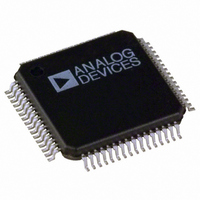
AD7656BSTZ-1 Analog Devices Inc, AD7656BSTZ-1 Datasheet - Page 29

AD7656BSTZ-1
Manufacturer Part Number
AD7656BSTZ-1
Description
6-CHANNEL 16-BIT SE BIPOLAR I.C.
Manufacturer
Analog Devices Inc
Specifications of AD7656BSTZ-1
Number Of Bits
16
Sampling Rate (per Second)
250k
Data Interface
Serial, Parallel
Number Of Converters
6
Power Dissipation (max)
143mW
Voltage Supply Source
Analog and Digital, Dual ±
Operating Temperature
-40°C ~ 85°C
Mounting Type
Surface Mount
Package / Case
64-LQFP
Lead Free Status / RoHS Status
Lead free / RoHS Compliant
For Use With
EVAL-AD7656-1EDZ - BOARD EVAL CONTROL AD7656-1EVAL-AD7656-1CBZ - BOARD EVAL FOR AD7656-1EVAL-AD7656CBZ - BOARD EVAL FOR AD7656
Lead Free Status / RoHS Status
Lead free / RoHS Compliant
Available stocks
Company
Part Number
Manufacturer
Quantity
Price
Company:
Part Number:
AD7656BSTZ-1
Manufacturer:
ADI
Quantity:
3
Company:
Part Number:
AD7656BSTZ-1
Manufacturer:
Analog Devices Inc
Quantity:
10 000
Part Number:
AD7656BSTZ-1
Manufacturer:
ADI/亚德诺
Quantity:
20 000
Company:
Part Number:
AD7656BSTZ-1-RL
Manufacturer:
Analog Devices Inc
Quantity:
10 000
APPLICATION HINTS
LAYOUT
The printed circuit board that houses the AD7656-1/AD7657-1/
AD7658-1 should be designed so that the analog and digital
sections are separated and confined to different areas of the board.
At least one ground plane should be used. It can be common or
split between the digital and analog sections. In the case of the
split plane, the digital and analog ground planes should be
joined in only one place, preferably underneath the AD7656-1/
AD7657-1/AD7658-1, or at least as close as possible to the part.
If the AD7656-1/AD7657-1/AD7658-1 are in a system where
multiple devices require analog-to-digital ground connections,
the connection should still be made at only one point, a star
ground point, which should be established as close as possible to
the AD7656-1/AD7657-1/AD7658-1. Good connections should
be made to the ground plane. Avoid sharing one connection for
multiple ground pins. Individual vias or multiple vias to the
ground plane should be used for each ground pin.
Avoid running digital lines under the devices because doing so
couples noise onto the die. The analog ground plane should be
allowed to run under the AD7656-1/AD7657-1/AD7658-1 to
avoid noise coupling. Fast-switching signals like CONVST or
clocks should be shielded with digital ground to avoid radiating
noise to other sections of the board, and they should never run
near analog signal paths. Crossover of digital and analog signals
should be avoided. Traces on layers in close proximity on the
board should run at right angles to each other to reduce the
effect of feedthrough through the board.
The power supply lines to the AV
on the AD7656-1/AD7657-1/AD7658-1 should use as large a
trace as possible to provide low impedance paths and reduce the
CC
, DV
CC
, V
DRIVE
, V
DD
, and V
SS
pins
Rev. 0 | Page 29 of 32
effect of glitches on the power supply lines. Good connections
should be made between the AD7656-1/AD7657-1/AD7658-1
supply pins and the power tracks on the board; this should involve
the use of a single via or multiple vias for each supply pin.
Good decoupling is also important to lower the supply impedance
presented to the AD7656-1/AD7657-1/AD7658-1 and to reduce
the magnitude of the supply spikes. The decoupling capacitors
should be placed close to, ideally right up against, these pins
and their corresponding ground pins. Additionally, low-ESR
1 μF capacitors should be placed on each of the supply pins, the
REFIN/REFOUT pin, and each REFCAPx pin. Avoid sharing
these capacitors between pins, and use vias to connect the
capacitors to the power and ground planes. In addition, use
wide, short traces between each via and the capacitor pad, or
place the vias adjacent to the capacitor pad to minimize parasitic
inductances. The AD7656-1/AD7657-1/AD7658-1 offer the user
a reduced decoupling solution that is pin and software compatible
with AD7656/AD7657/AD7658. The recommended reduced
decoupling required for AD7656-1/AD7657-1/AD7658-1 is
outlined in Figure 27.
Figure 27 shows an external Schmitt trigger device on the
CONVST A, CONVST B, CONVST C inputs. The Schmitt trigger
can be placed close to the CONVST pins (decoupled to the digital
ground) and is used to eliminate any system noise that couples onto
long CONVST A, CONVST B, CONVST C traces from being
applied to the CONVST pins. The Schmitt trigger offers noise
immunity to any high frequency noise, providing a clean
conversion edge to the AD7656-1/AD7657-1/AD7658-1 device in
cases where there is large system noise capable of coupling onto the
CONVST trace.
AD7656-1/AD7657-1/AD7658-1


