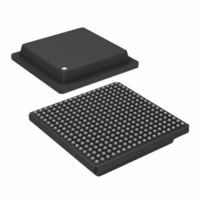
AD6635BB Analog Devices Inc, AD6635BB Datasheet - Page 54

AD6635BB
Manufacturer Part Number
AD6635BB
Description
IC,RF/Baseband Circuit,CMOS,BGA,324PIN,PLASTIC
Manufacturer
Analog Devices Inc
Series
AD6635r
Datasheet
1.AD6635BBPCB.pdf
(60 pages)
Specifications of AD6635BB
Rohs Status
RoHS non-compliant
Rf Type
Cellular, CDMA2000, EDGE, GPRS, GSM
Number Of Mixers
1
Current - Supply
880mA
Voltage - Supply
3 V ~ 3.6 V
Package / Case
324-BGA
Frequency
-
Gain
-
Noise Figure
-
Secondary Attributes
-
Lead Free Status / RoHS Status
Available stocks
Company
Part Number
Manufacturer
Quantity
Price
Part Number:
AD6635BB
Manufacturer:
ADI/亚德诺
Quantity:
20 000
AD6635
A[2:0] Name
111
110
101
100
011
010
001
000
Access Control Register (ACR)
The access control register serves to define the channel or
channels that receive an access from the microport or serial
port control.
Bit 7 of this register is the Auto-Increment bit. If this bit is 1,
the CAR register described below will increment its value after
every read/write access to the channel. It essentially means that
CAR (external address 6) need not be written for every memory
access, and the user can write to DR2, DR1, DR0 continuously
Access Control
Register (ACR)
Channel Address
Register (CAR)
SOFT_SYNC Control
Register (Write Only)
PIN_SYNC Control
Register (Write Only)
SLEEP (Write Only)
Data Register 2 (DR2)
Data Register 1 (DR1)
Data Register 0 (DR0)
Table XVI. External Memory Map
Comment
7:
6:
5–2: Instruction[3:0]
1–0: A[9:8]
7–0: A[7:0]
7:
6:
5:
4:
3:
2:
1:
0:
7:
6:
5:
4:
3:
2:
1:
0:
7–6: Reserved (low)
5:
Control Registers
4:
3:
2:
1:
0:
7–4: Reserved
3–0: D[19:16]
15–8: D[15:8]
7–0: D[7:0]
Auto Increment
Broadcast
PN_EN
Test_MUX_Select
Hop
Start
SYNC 3
SYNC 2
SYNC 1
SYNC 0
Toggle IEN for BIST
First SYNC Only
Hop_En
Start_En
SYNC_EN A
SYNC_EN B
SYNC_EN C
SYNC_EN D
Access Input/Output Port
Reserved low
SLEEP 3
SLEEP 2
SLEEP 1
SLEEP 0
–54–
while accessing consecutive memory location in each access.
This allows blocks of address space such as coefficient memory
to be initialized more efficiently.
Bit 6 of the register is the Broadcast bit and determines how
Bits 5–2 are interpreted. If Broadcast is 0, then Bits 4–2, which
are referred to as Instruction bits (Instruction[2:0]), are com-
pared with the CHIPn_ID[2:0] pins (n = 0 when /CS0 is used,
and n = 1 when /CS1 is used). The instruction that matches the
CHIPn_ID[2:0] pins will determine the access. This allows up
to two chips to be connected to the same port and their
memory to be mapped without external logic. This also allows
the same serial port of a host processor to configure up to eight
chips. If the Broadcast bit is high, the Instruction[3:0] word
allows multiple AD6635 channels and/or chips to be configured
simultaneously, independent of the CHIPn_ID[2:0] pins. There
are seven possible instructions that are defined in the table
below. This is useful for smart antenna systems in which mul-
tiple channels listening to a single antenna or carrier can be
configured simultaneously. An x in the table represents “don’t
care” in the digital decoding.
Instruction
0000
0001
0010
0100
1000
1100
1110
*A[9:8] bits control which channel is decoded for the access.
Note that CHIP0_ID[2:0] is used when CS0 is used for
programming. CHIP1_ID[2:0] is used when CS1 is used
for programming.
When broadcast is enabled (Bit 6 set high), the readback is not
valid because of the potential for internal bus contention. There-
fore, if readback is subsequently desired, the broadcast bit should
be set low.
Bits 1–0 of this register are address bits that decode which of
the four channels are being accessed, i.e., Channels 0–3 when
CS0 is used, and similarly, Channels 4–7 when CS1 is used. If
the Instruction bits decode an access to multiple channels, these
bits are ignored. If the Instruction decodes an access to a subset
of chips, the A[9:8] bits will otherwise determine the channel
being accessed. It should be noted that if access to input/output
control registers (Bit 5 of external address 3) is set, then A[9:8]
are not decoded.
Channel Address Register (CAR)
This register represents the 8-bit internal address of each chan-
nel. If the Auto-Increment bit of the ACR is 1, this value will be
incremented after every access to the DR0 register, which will
Table XVII. Microport Instructions
Comment
All Chips and All Channels Get Access
Channel 0,1,2 of All Chips Get Access
Channel 1,2,3 of All Chips Get Access
All Chips Get Access*
All Chips with CHIPn_ID[2:0] = xxx Get
Access* (same as previous instruction)
All Chips with CHIPn_ID[2:0] = xx0 Get
Access*
All Chips with CHIPn_ID[2:0] = xx1 Get
Access*
REV. 0


