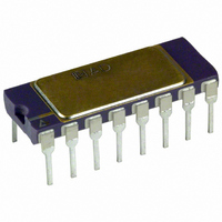
AD625AD Analog Devices Inc, AD625AD Datasheet - Page 14

AD625AD
Manufacturer Part Number
AD625AD
Description
Instrumentation Amplifier IC
Manufacturer
Analog Devices Inc
Datasheet
1.AD625KNZ.pdf
(15 pages)
Specifications of AD625AD
Gain Max, V/v
10000
Input Offset Voltage Max
200V
Supply Voltage Max
18V
Mounting Type
Through Hole
Supply Voltage Min
6V
Gain Min, V/v
1
Package / Case
16-CDIP
Rohs Status
RoHS non-compliant
Amplifier Type
Instrumentation
Number Of Circuits
1
Slew Rate
5 V/µs
Gain Bandwidth Product
25MHz
-3db Bandwidth
650kHz
Current - Input Bias
30nA
Voltage - Input Offset
50µV
Current - Supply
3.5mA
Voltage - Supply, Single/dual (±)
±6 V ~ 18 V
Operating Temperature
-40°C ~ 85°C
Output Type
-
Current - Output / Channel
-
Lead Free Status / RoHS Status
Available stocks
Company
Part Number
Manufacturer
Quantity
Price
Company:
Part Number:
AD625ADZ
Manufacturer:
AKM
Quantity:
1 400
Company:
Part Number:
AD625ADZ
Manufacturer:
Analog Devices Inc
Quantity:
135
AD625
DETERMINING SPGA RESISTOR NETWORK VALUES
The individual resistors in the gain network can be calculated
sequentially using the formula given below. The equation deter-
mines the resistors as labeled in Figure 41. The feedback resis-
tors and the gain setting resistors are interactive, therefore; the
formula must be a series where the present term is dependent on
the preceding term(s). The formula
can be used to calculate the necessary feedback resistors for any
set of gains. This formula yields a network with a total resistance
of 40 kΩ. A dummy variable (j) serves as a counter to keep a
running total of the preceding feedback resistors. To illustrate
how the formula can be applied, an example similar to the
calculation used for the resistor network in Figure 38 is exam-
ined below.
1) Unity gain is treated as a separate case. It is implemented
2) Before making any calculations it is advised to draw a resistor
with separate 20 kΩ feedback resistors as shown in Figure 41.
It is then ignored in further calculations.
network similar to the network in Figure 41. The network
will have (2 × M) + 1 resistors, where M = number of gains.
For Figure 38 M = 3 (4, 16, 64), therefore, the resistor string
will have seven resistors (plus the two 20 kΩ “side” resistors
for unity gain).
1000
800
400
200
100
R
80
40
20
10
8
4
2
1
F i
1
+
1
=
(
20
4
k
Ω
–
16
∑
j
1
=
0
R
R
ON
F j
GAIN
64
= 500
) ( –
1
R
ON
G
R
256
G
ON
= 1k
i
=
i
1
= 0
)
R
ON
1024
G
R
= 200
0
F
0
=
=
1
4096
0
3) Begin all calculations with G
4) The center resistor (R
5) If different resistor values are desired, all the resistors in the
6) Round off errors can be cumulative, therefore, it is advised to
TO GAIN SENSE
R
R
mined last. Its value is the remaining resistance of the 40 kΩ
string, and can be calculated with the equation:
network can be scaled by some convenient factor. However,
raising the impedance will increase the RTO errors, lowering
the total network resistance below 20 kΩ can result in ampli-
fier instability. More information on this phenomenon is
given in the RPGA section of the data sheet. The scale factor
will not affect the unity gain feedback resistors. The resistor
network in Figure 38 has a scaling factor of 650/625 = 1.04,
if this factor is used on R
tor values will match exactly.
carry as many significant digits as possible until all the values
have been calculated.
R
(PIN 2)
F 1
F 2
F 3
CONNECT IF UNITY
GAIN IS DESIRED
= (20 kΩ – R
= [20 kΩ – (R
= [20 kΩ – (R
R
R
20k
F 0
F 0
R
+ R
+ R
AD75xx
G
TO GAIN DRIVE
= 40 k Ω – 2 (R
(PIN 5)
F 1
F 1
= 15 kΩ ∴ R
+ R
RF
RF
R
40 k Ω – 39.375 k Ω = 625 Ω
F 0
F 0
1
G
2
F 0
) (1–1/4): R
+ R
F 2
=
+ R
G
(
= 18.75 kΩ ∴ R
of the highest gain setting), is deter-
40
RF
F 1
F 1
F 1
N
)] (1–4/16):
, R
k
+ R
F 0
RF
0
Ω
F 2
G
F 2
= 1 and R
+ R
F 0
–
F 2
= 3.75 kΩ
, R
RF
2
)] (1–16/64):
= 0 ∴ R
N
F 1
∑
j
F 3
M
=
, and R
0
+ R
R
TO GAIN DRIVE
F j
F 3
F 0
RF
F 2
(PIN 12)
)
F 1
2
= 937.5 Ω
= 0.
+ R
G
CONNECT IF UNITY
= 15 kΩ
GAIN IS DESIRED
, then the resis-
F 3
)
20k
TO GAIN SENSE
(PIN 15)


