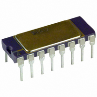
AD625AD Analog Devices Inc, AD625AD Datasheet - Page 13
AD625AD
Manufacturer Part Number
AD625AD
Description
Instrumentation Amplifier IC
Manufacturer
Analog Devices Inc
Datasheet
1.AD625KNZ.pdf
(15 pages)
Specifications of AD625AD
Gain Max, V/v
10000
Input Offset Voltage Max
200V
Supply Voltage Max
18V
Mounting Type
Through Hole
Supply Voltage Min
6V
Gain Min, V/v
1
Package / Case
16-CDIP
Rohs Status
RoHS non-compliant
Amplifier Type
Instrumentation
Number Of Circuits
1
Slew Rate
5 V/µs
Gain Bandwidth Product
25MHz
-3db Bandwidth
650kHz
Current - Input Bias
30nA
Voltage - Input Offset
50µV
Current - Supply
3.5mA
Voltage - Supply, Single/dual (±)
±6 V ~ 18 V
Operating Temperature
-40°C ~ 85°C
Output Type
-
Current - Output / Channel
-
Lead Free Status / RoHS Status
Available stocks
Company
Part Number
Manufacturer
Quantity
Price

Company:
Part Number:
AD625ADZ
Manufacturer:
AKM
Quantity:
1 400
Company:
Part Number:
AD625ADZ
Manufacturer:
Analog Devices Inc
Quantity:
135


These capacitances may also be incorporated as part of the
external input protection circuit (see section on Input Protec-
tion). As a general practice every effort should be made to
match the extraneous capacitance at Pins 15 and 2, and Pins 1
and 16, to preserve high ac CMR.
SOFTWARE PROGRAMMABLE GAIN AMPLIFIER
An SPGA provides the ability to externally program precision
gains from digital inputs. Historically, the problem in systems
requiring electronic switching of gains has been the ON resis-
tance (R
gain setting resistor R
and gain drifts. The AD625 eliminates this problem by making
the gain drive and gain sense pins available (Pins 2, 15, 5, 12;
see Figure 39). Consequently the multiplexer’s ON resistance is
removed from the signal current path. This transforms the ON
resistance error into a small nullable offset error. To clarify this
point, an error budget analysis has been performed in Table II
based on the SPGA configuration shown in Figure 39.
Figure 38 shows an AD625 based SPGA with possible gains of
1, 4, 16, 64. R
lines (Pins 2 and 15) of the AD625. In Figure 38, R
the sum of the two 975 Ω resistors and the 650 Ω resistor, or
2600 Ω. R
gain drive pins (Pins 12 and 15, or Pins 2 and 5), that is R
equals the 15.6 kΩ resistor plus the 3.9 kΩ resistor, or 19.5 kΩ.
The gain, therefore equals:
As the switches of the differential multiplexer proceed synchro-
nously, R
gain settings.
GND
V
V
DD
SS
ON
G
AD7502
F
) of the multiplexer, which appears in series with the
and R
20k
+GAIN DRIVE
equals the resistance between the gain sense and the
+V
RTI NULL
RTI NULL
SENSE
S
G
+GAIN
equals the resistance between the gain sense
F
REF
2R
–V
NC
R
change, resulting in the various programmed
TTL/DTL TO CMOS LEVEL TRANSLATOR
S
G
F
15.6k
3.9k
1
2
3
4
5
6
7
8
G
+INPUT
. This can result in substantial gain errors
+1=
AD625
10k
975
DECODER/DRIVER
10k
2(19.5 kΩ)
A1
(2.6 kΩ)
650
A3
10k
A2
10k
975
–INPUT
15.6k
3.9k
+1=16
16
15
14
13
12
11
10
9
RTO NULL
RTO NULL
–GAIN DRIVE
+V
–GAIN
SENSE
S
V
20k
–V
OUT
S
G
equals
F
A0
A1
E
N
Figure 39 shows a complete SPGA feeding a 12-bit DAS with a
0 V–10 V input range. This configuration was used in the error
budget analysis shown in Table II. The gain used for the RTI
calculations is set at 16. As the gain is changed, the ON resis-
tance of the multiplexer and the feedback resistance will change,
which will slightly alter the values in the table.
Induced
Error
RTI Offset
Voltage
RTI Offset
Voltage
RTO Offset Feedback
Voltage
RTO Offset Feedback
Voltage
Total error induced by a typical CMOS multiplexer
to an SPGA at +25°C
NOTES
**The frequency response and settling will be affected by the ON resistance and
**Switch resistance and leakage current errors can be reduced by using relays.
V
–
+
1
2
IN
The resistor for this calculation is the user-provided feedback resistance (R
The leakage currents (I
20 kΩ is recommended value (see Resistor Programmable Gain Amplifier section).
will be determined by the difference between the leakages of each “half’’ of the
differential multiplexer. The differential leakage current is multiplied by the
feedback resistance (see Note 1), to determine offset voltage. Because differential
leakage current is not a parameter specified on multiplexer data sheets, the most
extreme difference (one most positive and one most negative) was used for the
calculations in Table II. Typical performance will be much better.
internal capacitance of the multiplexer. Figure 40 shows the settling time vs.
ON resistance at different gain settings for an AD625 based SPGA.
Table II. Errors Induced by Multiplexer to an SPGA
C
C
OUT
OUT
AD625C
Gain Sense Switch
Offset
Current
40 nA
Gain Sense Differential
Current
60 nA
Resistance Leakage
20 kΩ
Resistance Leakage
20 kΩ
I
I
OUT
OUT
R
R
C
C
ON
ON
S-OUT
S-OUT
Specifications
1
1
I
I
S
S
S
and I
C
C
AD7520KN Calculation
Resistance
170 Ω
Switch
Resistance
6.8 Ω
Differential
Current (I
+0.2 nA
–0.2 nA
Differential
Current
(I
+1 nA
–1 nA
S
S
OUT
OUT
15.6k
15.6k
20k
20k
3.9k
975k
650k
975k
3.9k
) will induce an offset voltage, however, the offset
)
2
–INPUT
+INPUT
SENSE
SENSE
S
–GAIN
+GAIN
–GAIN
DRIVE
+GAIN
DRIVE
)
2
40 nA × 170 Ω =
6.8 µV
60 nA × 6.8 Ω =
0.41 µV
2 (0.2 nA × 20 kΩ)
= 8 µV/16
2 (1 nA × 20 kΩ)
= 40 µV/16
V
S
10k
10k
AD625
AD625
10k
10k
Voltage Offset
Induced RTI
6.8 µV
0.41 µV
0.5 µV
2.5 µV
10.21 A
F
).
12-BIT
DAS
Related parts for AD625AD
Image
Part Number
Description
Manufacturer
Datasheet
Request
R

Part Number:
Description:
DPG2 EVAL ADAPTER FOR XILINX BOARDS
Manufacturer:
Analog Devices Inc
Part Number:
Description:
Xilinx FMC Interface
Manufacturer:
Analog Devices Inc
Datasheet:
Part Number:
Description:
Xilinx FMC Interface
Manufacturer:
Analog Devices Inc
Datasheet:
Part Number:
Description:
Xilinx FMC Interface
Manufacturer:
Analog Devices Inc
Datasheet:
Part Number:
Description:
Xilinx FMC Interface
Manufacturer:
Analog Devices Inc
Datasheet:
Part Number:
Description:
Xilinx FMC Interface
Manufacturer:
Analog Devices Inc
Datasheet:
Part Number:
Description:
Xilinx FMC Interface
Manufacturer:
Analog Devices Inc
Datasheet:
Part Number:
Description:
Xilinx FMC Interface
Manufacturer:
Analog Devices Inc
Datasheet:
Part Number:
Description:
AD CONVERTOR, IC, BIT COUNT FOR PROCESSOR
Manufacturer:
Analog Devices Inc

Part Number:
Description:
±1.7g Dual-Axis IMEMS Accelerometer Evaluation Board
Manufacturer:
Analog Devices Inc
Datasheet:
Part Number:
Description:
Inertial Sensor Evaluation System
Manufacturer:
Analog Devices Inc
Datasheet:
Part Number:
Description:
Manufacturer:
Analog Devices Inc
Datasheet: