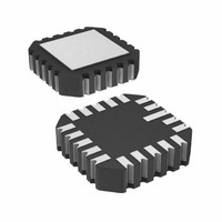
AD585SE Analog Devices Inc, AD585SE Datasheet - Page 4

AD585SE
Manufacturer Part Number
AD585SE
Description
IC,Sample/Track-and-Hold Amplifier,SINGLE,BIPOLAR/JFET,LLCC,20PIN,CERAMIC
Manufacturer
Analog Devices Inc
Datasheet
1.AD585JPZ-REEL7.pdf
(6 pages)
Specifications of AD585SE
Rohs Status
RoHS non-compliant
Amplifier Type
Sample and Hold
Number Of Circuits
1
Slew Rate
10 V/µs
-3db Bandwidth
2MHz
Current - Input Bias
2nA
Voltage - Input Offset
2000µV
Current - Supply
10mA
Current - Output / Channel
50mA
Voltage - Supply, Single/dual (±)
±5 V ~ 18 V
Operating Temperature
-55°C ~ 125°C
Mounting Type
Surface Mount
Package / Case
20-CLCC
Output Type
-
Gain Bandwidth Product
-
Lead Free Status / RoHS Status
Available stocks
Company
Part Number
Manufacturer
Quantity
Price
AD585
SAMPLED DATA SYSTEMS
In sampled data systems there are a number of limiting factors
in digitizing high frequency signals accurately. Figure 9 shows
pictorially the sample-and-hold errors that are the limiting fac-
tors. In the following discussions of error sources the errors will
be divided into the following groups: 1. Sample-to-Hold Transi-
tion, 2. Hold Mode and 3. Hold-to-Sample Transition.
SAMPLE-TO-HOLD TRANSITION
The aperture delay time is the time required for the sample-and-
hold amplifier to switch from sample to hold. Since this is effec-
tively a constant then it may be tuned out. If however, the
aperture delay time is not accounted for then errors of the mag-
nitude as shown in Figure 10 will result.
To eliminate the aperture delay as an error source the sample-
to-hold command may be advanced with respect to the input
signal .
Once the aperture delay time has been eliminated as an error
source then the aperture jitter which is the variation in aperture
delay time from sample-to-sample remains. The aperture jitter is
a true error source and must be considered. The aperture jitter
is a result of noise within the switching network which modu-
lates the phase of the hold command and is manifested in the
variations in the value of the analog input that has been held.
The aperture error which results from this jitter is directly re-
lated to the dV/dT of the analog input.
The error due to aperture jitter is easily calculated as shown be-
low. The error calculation takes into account the desired accu-
racy corresponding to the resolution of the N-bit A/D converter.
Figure 9. Pictorial Showing Various S/H Characteristics
Figure 10. Aperture Delay Error vs. Frequency
–4–
For an application with a 10-bit A/D converter with a 10 V full
scale to a 1/2 LSB error maximum.
For an application with a 12-bit A/D converter with a 10 V full
scale to a 1/2 LSB error maximum:
Figure 11 shows the entire range of errors induced by aperture
jitter with respect to the input signal frequency.
Sample-to-hold offset is caused by the transfer of charge to the
holding capacitor via the gate capacitance of the switch when
switching into hold. Since the gate capacitance couples the
switch control voltage applied to the gate on to the hold capaci-
tor, the resulting sample-to-hold offset is a function of the logic
level .
The logic inputs were designed for application flexibility and,
therefore, a wide range of logic thresholds. This was achieved by
using a differential input stage for HOLD and HOLD. Figure 1
shows the change in the sample-to-hold offset voltage based
upon an independently programmed reference voltage. Since
the input stage is a differential configuration, the offset voltage
is a function of the control voltage range around the pro-
grammed threshold voltage.
The sample-to-hold offset can be reduced by adding capacitance
to the internal 100 pF capacitor and by using HOLD instead of
HOLD. This may be easily accomplished by adding an external
capacitor between Pins 7 and 8. The sample-to-hold offset is
then governed by the relationship:
Figure 11. Aperture Jitter Error vs. Frequency
S/H Offset (V )
f
MAX
f
f
f
f
MAX
MAX
MAX
MAX
77.7 kHz.
( Aperture Jitter )
310.8 kHz.
(0.5 10
(0.5 10
2
2
2
C
–(10 1)
–(12 1)
–( N
Charge pC
H
Total ( pF )
1)
–9
–9
)
)
REV. A


