AD585SE Analog Devices Inc, AD585SE Datasheet - Page 2
AD585SE
Manufacturer Part Number
AD585SE
Description
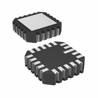
IC,Sample/Track-and-Hold Amplifier,SINGLE,BIPOLAR/JFET,LLCC,20PIN,CERAMIC
Manufacturer
Analog Devices Inc
Datasheet
1.AD585JPZ-REEL7.pdf
(6 pages)
Specifications of AD585SE
Rohs Status
RoHS non-compliant
Amplifier Type
Sample and Hold
Number Of Circuits
1
Slew Rate
10 V/µs
-3db Bandwidth
2MHz
Current - Input Bias
2nA
Voltage - Input Offset
2000µV
Current - Supply
10mA
Current - Output / Channel
50mA
Voltage - Supply, Single/dual (±)
±5 V ~ 18 V
Operating Temperature
-55°C ~ 125°C
Mounting Type
Surface Mount
Package / Case
20-CLCC
Output Type
-
Gain Bandwidth Product
-
Lead Free Status / RoHS Status
Available stocks
Company
Part Number
Manufacturer
Quantity
Price


AD585–SPECIFICATIONS
Model
SAMPLE/HOLD CHARACTERISTICS
TRANSFER CHARACTERISTICS
ANALOG INPUT CHARACTERISTICS
DIGITAL INPUT CHARACTERISTICS
POWER SUPPLY CHARACTERISTICS
TEMPERATURE RANGE
PACKAGE OPTIONS
NOTES
1
2
3
4
Maximum input signal is the minimum supply minus a headroom voltage of 2.5 V.
Not tested at –55 C.
E = Leadless Ceramic Chip Carrier; P = Plastic Leaded Chip Carrier; Q = Cerdip.
For AD585/883B specifications, refer to Analog Devices Military Products Databook.
Acquisition Time, 10 V Step to 0.01%
Aperture Time, 20 V p-p Input,
Aperture Jitter, 20 V p-p Input,
Settling Time, 20 V p-p Input,
Droop Rate
Droop Rate T
Charge Transfer
Feedthrough
Open Loop Gain
Application Resistor Mismatch
Common-Mode Rejection
Small Signal Gain Bandwidth
Full Power Bandwidth
Slew Rate
Output Resistance (Sample Mode)
Output Short Circuit Current
Output Short Circuit Duration
Offset Voltage
Offset Voltage, T
Bias Current
Bias Current, T
Input Capacitance, f = 1 MHz
Input Resistance, Sample or Hold
TTL Reference Output
Logic Input High Voltage
Logic Input Low Voltage
Logic Input Current (Either Input)
Operating Voltage Range
Supply Current, R
Power Supply Rejection, Sample Mode
Specified Performance
Cerdip (Q-14)
LCC (E-20A)
PLCC (P-20A)
HOLD 0 V
HOLD 0 V
HOLD 0 V, to 0.01%
Sample-to-Hold Offset
20 V p-p, 10 kHz Input
V
V
V
V
V
I
20 V p-p Input, A = +1
T
T
OUT
OUT
CM
OUT
OUT
OUT
MIN
MIN
= 10 V
= 10 mA
= 20 V p-p
to T
to T
= 20 V p-p, R
= 100 mV p-p
= 20 V p-p
MAX
MAX
MIN
MIN
MIN
to T
L
20 V Step to 0.01%
to T
=
3, 4
to T
L
MAX
= 2k
MAX
MAX
1
Min
–3
80
1.2
2.0
+5, –10.8
6
70
0
Doubles Every 10 C
Indefinite
AD585JP
AD585J
Typ
35
0.5
0.5
0.5
200,000
2.0
160
10
50
10
10
1.4
(typical @ +25 C and V
HOLD active unless otherwise noted)
12
Max
3
5
1
0.3
3
0.3
0.05
5
6
2
5
1.6
0.8
50
10
+70
18
–2–
Min
–3
80
1.2
2.0
+5, –10.8
6
70
–25
Double Every 10 C
Specifications subject to change without notice.
Specifications shown in boldface are tested on all production units at final electrical
test. Results from those tests are used to calculate outgoing quality levels.
All min and max specifications are
boldface are tested on all production units.
Indefinite
AD585AQ
AD585A
S
=
0.5
Typ
35
0.5
0.5
200,000
2.0
160
10
50
10
10
1.4
12
12 V or 15 V, and C
Max
3
5
1
0.3
3
0.3
0.05
2
3
2
5
1.6
0.8
50
10
+85
18
–3
Min
80
1.2
2.0
+5, –10.8
6
70
–55
Doubles Every 10 C
AD585SQ
AD585SE
guaranteed, although only those shown in
Indefinite
H
AD585S
= Internal, A = +1,
Typ
35
0.5
0.5
0.5
200,000
2.0
160
10
50
20
10
10
1.4
12
0.3
3
0.3
Max
3
5
1
0.05
2
3
2
50
1.6
0.7
50
10
+125
18
2
Units
ns
ns
mV/ms
pC
mV
mV
V/V
%
dB
MHz
kHz
V/ s
mA
mV
mV
nA
nA
pF
V
V
V
V
mA
dB
C
s
s
s
A
REV. A
Related parts for AD585SE
Image
Part Number
Description
Manufacturer
Datasheet
Request
R

Part Number:
Description:
DPG2 EVAL ADAPTER FOR XILINX BOARDS
Manufacturer:
Analog Devices Inc
Part Number:
Description:
Xilinx FMC Interface
Manufacturer:
Analog Devices Inc
Datasheet:
Part Number:
Description:
Xilinx FMC Interface
Manufacturer:
Analog Devices Inc
Datasheet:
Part Number:
Description:
Xilinx FMC Interface
Manufacturer:
Analog Devices Inc
Datasheet:
Part Number:
Description:
Xilinx FMC Interface
Manufacturer:
Analog Devices Inc
Datasheet:
Part Number:
Description:
Xilinx FMC Interface
Manufacturer:
Analog Devices Inc
Datasheet:
Part Number:
Description:
Xilinx FMC Interface
Manufacturer:
Analog Devices Inc
Datasheet:
Part Number:
Description:
Xilinx FMC Interface
Manufacturer:
Analog Devices Inc
Datasheet:
Part Number:
Description:
AD CONVERTOR, IC, BIT COUNT FOR PROCESSOR
Manufacturer:
Analog Devices Inc

Part Number:
Description:
±1.7g Dual-Axis IMEMS Accelerometer Evaluation Board
Manufacturer:
Analog Devices Inc
Datasheet:
Part Number:
Description:
Inertial Sensor Evaluation System
Manufacturer:
Analog Devices Inc
Datasheet:
Part Number:
Description:
Manufacturer:
Analog Devices Inc
Datasheet: