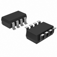
AD5620BRJZ-1500RL7 Analog Devices Inc, AD5620BRJZ-1500RL7 Datasheet - Page 19

AD5620BRJZ-1500RL7
Manufacturer Part Number
AD5620BRJZ-1500RL7
Description
IC,D/A CONVERTER,SINGLE,12-BIT,CMOS,TSSOP,8PIN
Manufacturer
Analog Devices Inc
Series
nanoDAC™r
Datasheet
1.AD5620ARJZ-1500RL7.pdf
(28 pages)
Specifications of AD5620BRJZ-1500RL7
Design Resources
Single-Ended-to-Differential Converters for Voltage Output and Current Output DACs Using AD8042 (CN0143) Amplitude Control Circuit for AD9834 Waveform Generator (CN0156)
Settling Time
8µs
Number Of Bits
12
Data Interface
DSP, MICROWIRE™, QSPI™, Serial, SPI™
Number Of Converters
1
Voltage Supply Source
Single Supply
Power Dissipation (max)
2.5mW
Operating Temperature
-40°C ~ 105°C
Mounting Type
Surface Mount
Package / Case
SOT-23-8
Number Of Channels
1
Resolution
12b
Conversion Rate
125KSPS
Interface Type
Serial (3-Wire, SPI, QSPI, Microwire)
Single Supply Voltage (typ)
3V
Dual Supply Voltage (typ)
Not RequiredV
Architecture
Resistor-String
Power Supply Requirement
Single
Output Type
Voltage
Integral Nonlinearity Error
±1LSB
Single Supply Voltage (min)
2.7V
Single Supply Voltage (max)
3.3V
Dual Supply Voltage (min)
Not RequiredV
Dual Supply Voltage (max)
Not RequiredV
Operating Temp Range
-40C to 105C
Operating Temperature Classification
Industrial
Mounting
Surface Mount
Pin Count
8
Package Type
SOT-23
Lead Free Status / RoHS Status
Lead free / RoHS Compliant
Lead Free Status / RoHS Status
Lead free / RoHS Compliant
Other names
AD5620BRJZ-1500RL7TR
Available stocks
Company
Part Number
Manufacturer
Quantity
Price
Part Number:
AD5620BRJZ-1500RL7
Manufacturer:
ADI/亚德诺
Quantity:
20 000
POWER-ON RESET
The AD5620/AD5640/AD5660 family contains a power-on
reset circuit that controls the output voltage during power-up.
The AD5620/AD5640/AD5660-1-2 DAC output powers up to
0 V, and the AD5620/AD5660-3 DAC output powers up to
midscale. The output remains at this level until a valid write
sequence is made to the DAC, which is useful in applications
where it is important to know the state of the DAC output while
it is in the process of powering up.
POWER-DOWN MODES
The AD5620/AD5640/AD5660 have four separate modes of
operation. These modes are software-programmable by setting
two bits in the control register. Table 7 and Table 8 show how
the state of the bits corresponds to the operating mode of the
device.
Table 7. Modes of Operation for the AD5660
DB17
0
0
1
1
Table 8. Modes of Operation for the AD5620/AD5640
DB15
0
0
1
1
When both bits are set to 0, the part works normally with its
normal power consumption of 550 μA at 5 V. However, for the
three power-down modes, the supply current falls to 480 nA
at 5 V (200 nA at 3 V). Not only does the supply current fall,
but the output stage is internally switched from the output of
the amplifier to a resistor network of known values. The advan-
tage is that the output impedance of the part is known while the
part is in power-down mode. There are three options: the out-
put is connected internally to GND through a 1 kΩ or a 100 kΩ
resistor, or it is left open-circuited (three-stated). The output
stage is shown in Figure 44.
DB16
0
1
0
1
DB14
0
1
0
1
AD5660 Operating Mode
Normal operation
Power-down modes:
AD5620/AD5640 Operating Mode
Normal operation
Power-down modes:
1 kΩ to GND
100 kΩ to GND
Three-state
1 kΩ to GND
100 kΩ to GND
Three-state
Rev. F | Page 19 of 28
The bias generator, output amplifier, reference, resistor string,
and other associated linear circuitry are all shut down when
power-down mode is activated. However, the contents of the
DAC register are unaffected when in power-down. The time to
exit power-down is typically 5 μs for V
(see Figure 30).
MICROPROCESSOR INTERFACING
AD5660-to-Blackfin® ADSP-BF53x Interface
Figure 45 shows a serial interface between the AD5660 and the
Blackfin ADSP-BF53x microprocessor. The ADSP-BF53x
processor family incorporates two dual-channel synchronous
serial ports, SPORT1 and SPORT0, for serial and multi-
processor communications. Using SPORT0 to connect to the
AD5660, the setup for the interface is as follows: DT0PRI drives
the DIN pin of the AD5660, while TSCLK0 drives the SCLK of
the part and SYNC is driven from TFS0.
1
ADDITIONAL PINS OMITTED FOR CLARITY
ADSP-BF53x
STRING DAC
RESISTOR
Figure 45. AD5660-to-Blackfin ADSP-BF53x Interface
Figure 44. Output Stage During Power-Down
TSCLK0
DTOPRI
TFS0
1
POWER-DOWN
AMPLIFIER
AD5620/AD5640/AD5660
CIRCUITRY
DD
= 5 V and V
AD5660
SYNC
DIN
SCLK
NETWORK
RESISTOR
1
V
OUT
DD
= 3 V


