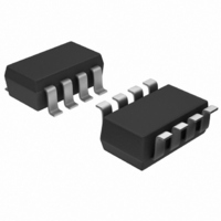
AD5620BRJZ-1500RL7 Analog Devices Inc, AD5620BRJZ-1500RL7 Datasheet - Page 18

AD5620BRJZ-1500RL7
Manufacturer Part Number
AD5620BRJZ-1500RL7
Description
IC,D/A CONVERTER,SINGLE,12-BIT,CMOS,TSSOP,8PIN
Manufacturer
Analog Devices Inc
Series
nanoDAC™r
Datasheet
1.AD5620ARJZ-1500RL7.pdf
(28 pages)
Specifications of AD5620BRJZ-1500RL7
Design Resources
Single-Ended-to-Differential Converters for Voltage Output and Current Output DACs Using AD8042 (CN0143) Amplitude Control Circuit for AD9834 Waveform Generator (CN0156)
Settling Time
8µs
Number Of Bits
12
Data Interface
DSP, MICROWIRE™, QSPI™, Serial, SPI™
Number Of Converters
1
Voltage Supply Source
Single Supply
Power Dissipation (max)
2.5mW
Operating Temperature
-40°C ~ 105°C
Mounting Type
Surface Mount
Package / Case
SOT-23-8
Number Of Channels
1
Resolution
12b
Conversion Rate
125KSPS
Interface Type
Serial (3-Wire, SPI, QSPI, Microwire)
Single Supply Voltage (typ)
3V
Dual Supply Voltage (typ)
Not RequiredV
Architecture
Resistor-String
Power Supply Requirement
Single
Output Type
Voltage
Integral Nonlinearity Error
±1LSB
Single Supply Voltage (min)
2.7V
Single Supply Voltage (max)
3.3V
Dual Supply Voltage (min)
Not RequiredV
Dual Supply Voltage (max)
Not RequiredV
Operating Temp Range
-40C to 105C
Operating Temperature Classification
Industrial
Mounting
Surface Mount
Pin Count
8
Package Type
SOT-23
Lead Free Status / RoHS Status
Lead free / RoHS Compliant
Lead Free Status / RoHS Status
Lead free / RoHS Compliant
Other names
AD5620BRJZ-1500RL7TR
Available stocks
Company
Part Number
Manufacturer
Quantity
Price
Part Number:
AD5620BRJZ-1500RL7
Manufacturer:
ADI/亚德诺
Quantity:
20 000
AD5620/AD5640/AD5660
INPUT SHIFT REGISTER
AD5620/AD5640
The input shift register is 16 bits wide for the AD5620/AD5640
(see Figure 40 and Figure 41). The first two bits are control bits
that control which mode of operation the part is in (normal
mode or any of the three power-down modes). The next
14/12 bits, respectively, are the data bits. These are transferred
to the DAC register on the 16
AD5660
The input shift register is 24 bits wide for the AD5660 (see
Figure 42). The first six bits are don’t care bits. The next two are
control bits that control which mode of operation the part is in
(normal mode or any of the three power-down modes). For a more
complete description of the various modes, see the Power-Down
Modes section. The next 16 bits are the data bits. These are
transferred to the DAC register on the 24
SYNC
SCLK
DB23 (MSB)
DIN
X
X
SYNC HIGH BEFORE 16
X
MSB
INVALID WRITE SEQUENCE:
DB15 (MSB)
DB15 (MSB)
PD1
PD1
X
th
X
PD0
PD0
falling edge of SCLK.
TH
/24
X
D13
D11
TH
FALLING EDGE
PD1
th
LSB
D12
D10
falling edge of SCLK.
PD0
D11
D9
D15
Figure 40. AD5620 Input Register Contents
Figure 41. AD5640 Input Register Contents
Figure 42. AD5660 Input Register Contents
D10
D8
Figure 43. SYNC Interrupt Facility
D14
D7
D9
Rev. F | Page 18 of 28
D13
DATA BITS
D6
D8
D12
DATA BITS
D5
D7
D10
SYNC INTERRUPT
In a normal write sequence for the AD5660, the SYNC line is
kept low for at least 24 falling edges of SCLK, and the DAC is
updated on the 24
high before the 24
write sequence. The shift register is reset, and the write sequence
is seen as invalid. Neither an update of the DAC register contents
nor a change in the operating mode occurs (see Figure 43).
Similarly, in a normal write sequence for the AD5620/AD5640,
the SYNC line is kept low for at least 16 falling edges of SCLK,
and the DAC is updated on the 16
SYNC is brought high before the 16
an interrupt to the write sequence.
D4
D6
D9
VALID WRITE SEQUENCE, OUTPUT UPDATES
D3
D5
DATA BITS
D8
ON THE 16
MSB
D2
D4
D7
D1
D3
th
th
TH
D6
/24
falling edge. However, if SYNC is brought
falling edge, this acts as an interrupt to the
TH
D0
D2
D5
FALLING EDGE
D1
X
D4
DB0 (LSB)
DB0 (LSB)
LSB
th
D0
D3
X
t
falling edge. However, if
h falling edge, this acts as
D2
D1
DB0 (LSB)
D0


