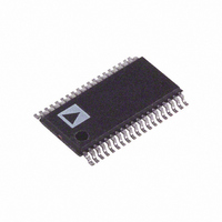
AD5557CRU-REEL7 Analog Devices Inc, AD5557CRU-REEL7 Datasheet - Page 9

AD5557CRU-REEL7
Manufacturer Part Number
AD5557CRU-REEL7
Description
IC,D/A CONVERTER,DUAL,14-BIT,TSSOP,38PIN
Manufacturer
Analog Devices Inc
Datasheet
1.AD5547BRUZ.pdf
(20 pages)
Specifications of AD5557CRU-REEL7
Design Resources
Precision, Unipolar, Inverting Conversion Using AD5547/57 DAC (CN0026) Precision, Unipolar, Noninverting Configuration for the AD5547/57 DAC (CN0027) Precision, Bipolar, Configuration for AD5547/AD5557 DAC (CN0028)
Settling Time
500ns
Number Of Bits
14
Data Interface
Parallel
Number Of Converters
2
Voltage Supply Source
Single Supply
Power Dissipation (max)
55µW
Operating Temperature
-40°C ~ 125°C
Mounting Type
Surface Mount
Package / Case
38-TSSOP
Lead Free Status / RoHS Status
Contains lead / RoHS non-compliant
Pin No.
23
24 to 28,
30 to 38
29
Table 5. Address Decoder Pins
A1
0
0
1
1
Table 6. Control Inputs
RS
0
1
1
1
1
1
WR
X
0
1
0
1
LDAC
X
0
1
1
0
Mnemonic
RS
D13 to D0
VDD
Register Operation
Reset the output to 0 with MSB = 0; reset the output to midscale with MSB = 1.
Load the input register with data bits.
Load the DAC register with the contents of the input register.
The input and DAC registers are transparent.
When LDAC and WR are tied together and programmed as a pulse, the data bits are loaded into the input register
on the falling edge of the pulse and are then loaded into the DAC register on the rising edge of the pulse.
No register operation.
A0
0
1
0
1
Function
Active low resets both input and DAC registers. Resets to zero-scale if MSB = 0 and resets to midscale if MSB =
1. Signal level must be ≤V
Digital Input Data Bits D13 to D0. Signal level must be ≤V
Positive Power Supply Input. The specified range of operation is 2.7 V to 5.5 V.
Output Update
DAC A
None
DAC A and DAC B
DAC B
DD
+ 0.3 V.
Rev. B | Page 9 of 20
DD
+ 0.3 V.
AD5547/AD5557


