AD53508JP Analog Devices Inc, AD53508JP Datasheet - Page 4
AD53508JP
Manufacturer Part Number
AD53508JP
Description
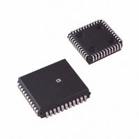
IC,ATE Circuit,LDCC,44PIN,PLASTIC
Manufacturer
Analog Devices Inc
Datasheet
1.AD53508JP.pdf
(8 pages)
Specifications of AD53508JP
Rohs Status
RoHS non-compliant
Applications
Testing Equipment
Interface
Analog
Voltage - Supply
14 V ~ 15.75 V
Package / Case
44-PLCC
Mounting Type
Surface Mount
Lead Free Status / RoHS Status
Available stocks
Company
Part Number
Manufacturer
Quantity
Price
Company:

Part Number:
AD53508JP
Manufacturer:
Analog Devices Inc
Quantity:
10 000


AD53508
CAUTION
ESD (electrostatic discharge) sensitive device. Electrostatic charges as high as 4000 V readily
accumulate on the human body and test equipment and can discharge without detection.
Although the AD53508 features proprietary ESD protection circuitry, permanent damage may
occur on devices subjected to high-energy electrostatic discharges. Therefore, proper ESD
precautions are recommended to avoid performance degradation or loss of functionality.
ABSOLUTE MAXIMUM RATINGS
(T
VDD to VEE
VCC to VEE
VDD to DGND
Digital Inputs to DGND –0.3
Power Dissipation
Operating Temperature
Storage Temperature
Lead Temperature
Force/Sense Outputs
Model
AD53508JP
nent damage to the device. These are stress ratings only; functional operation of
the device at these or any other conditions above those indicated in the operational
sections of this specification is not implied. Exposure to absolute maximum rating
conditions for extended periods may affect device reliability.
Stresses above those listed under Absolute Maximum Ratings may cause perma-
Range
A
FORCE EN A
DAC1 SEL A
MEAS OUT A
= 25°C unless otherwise noted)
FORCE I A
M CON A
GUARD A
FORCE A
SENSE A
R2 A
VCC
VEE
10
11
12
13
14
15
16
17
Temperature
Range
25°C to 70°C
7
8
9
PIN CONFIGURATION
18 19 20 21 22 23 24 25 26 27 28
6
ORDERING GUIDE
5
Min
–0.3
–0.3
–0.3
25
–60
VEE–0.8 VCC+0.8 V
4
(Not to Scale)
3
TOP VIEW
AD53508
2
1 44 43 42 41 40
Max
+26.4
+26.4
+6
VCC+0.3 V
700
+125
300
70
PIN 1
IDENTIFIER
Package
Description
Plastic Leaded
Chip Carrier
Unit Condition
V
V
V
mW
°C
°C
°C
39
38
37
36
35
34
33
32
31
30
29
Or 75 mA,
T
Soldering (10 sec)
Whichever Is Less
R2 B
SENSE B
FORCE B
GUARD B
MEAS OUT B
VDD
M CON B
DIGGND
FORCE I B
FORCE EN B
DAC1 SEL B
A
= ACTIVE LO
≤ 75°C
Package
Option
P-44A
Pin Name
1
2
3
4
5
6
7
8
9
10
11
12
13
14
15
16
17
18
19
20
21
22
23
24
25
26
27
28
29
30
31
32
33
34
35
36
37
38
39
40
41
42
43
44
= Active Lo
DSR_2.5
DAC2_A
DAC1_A
EXT_RC_A
C1_A
R1_A
R2_A
SENSE_A
FORCE_A
GUARD_A
MEAS_OUT_A
VCC
M_CON_A
VEE
FORCE_I_A
FORCE_EN_A
DAC1_SEL_A
INTEG_A
HOLD_A
I_RANGE0_A
I_RANGE1_A
VERIFY
OUTPUT_CON_A
OUTPUT_CON_B
I_RANGE1_B
I_RANGE0_B
HOLD_B
INTEG_B
DAC1_SEL_B
FORCE_EN_B
FORCE_I_B
DIGGND
M_CON_B
VDD
MEAS_OUT_B
GUARD_B
FORCE_B
SENSE_B
R2_B
R1_B
C1_B
EXT_RC_B
DAC1_B
DAC2_B
PIN FUNCTION DESCRIPTIONS
Description
2.5 V Reference Input
First of Two Switchable Inputs
Second of Two Switchable Inputs
External R
External Capacitor
External Resistor
External Resistor
Sense Input
Force Output
Guard Drive Output
Measurement Output
+15 V Analog Supply
Connect Measure Output to Bus
–10 V Analog Supply
Force V (When Hi) or I (When Lo)
Control Input
Select DAC1 (When Lo) or DAC2
Control Input
Control Input
Select 2 mA Range (Active Lo)
Select 200 µA Range (Active Lo)
Measure Forced Voltage or Current
Connect Pin Drive (Active Lo)
Connect Pin Drive (Active Lo)
Select 200 µA Range (Active Lo)
Select 2 mA Range (Active Lo)
Control Input
Control Input
Select DAC1 (When Lo) or DAC2
Control Input
Force V (When Hi) or I (When Lo)
Digital Ground
Connect Measure Output to Bus
+5 V Digital Supply
Measurement Output
Guard Drive Output
Force Output
Sense Input
External Resistor
External Resistor
External Capacitor
External R
Second of Two Switchable Inputs
First of Two Switchable Inputs
WARNING!
S
S
and C Common
and C Common
ESD SENSITIVE DEVICE
Related parts for AD53508JP
Image
Part Number
Description
Manufacturer
Datasheet
Request
R

Part Number:
Description:
±1.7g Dual-Axis IMEMS Accelerometer Evaluation Board
Manufacturer:
Analog Devices Inc
Datasheet:

Part Number:
Description:
Inertial Sensor Evaluation System
Manufacturer:
Analog Devices Inc
Datasheet:
Part Number:
Description:
Manufacturer:
Analog Devices Inc
Datasheet:
Part Number:
Description:
Manufacturer:
Analog Devices Inc
Datasheet:
Part Number:
Description:
Manufacturer:
Analog Devices Inc
Datasheet:
Part Number:
Description:
Manufacturer:
Analog Devices Inc
Datasheet:
Part Number:
Description:
Manufacturer:
Analog Devices Inc
Datasheet:
Part Number:
Description:
Manufacturer:
Analog Devices Inc
Datasheet:
Part Number:
Description:
Manufacturer:
Analog Devices Inc
Datasheet:
Part Number:
Description:
Manufacturer:
Analog Devices Inc
Datasheet:
Part Number:
Description:
Manufacturer:
Analog Devices Inc
Datasheet:
Part Number:
Description:
Manufacturer:
Analog Devices Inc
Datasheet:
Part Number:
Description:
Manufacturer:
Analog Devices Inc
Datasheet: