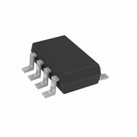
AD5227BUJZ100-R2 Analog Devices Inc, AD5227BUJZ100-R2 Datasheet - Page 11

AD5227BUJZ100-R2
Manufacturer Part Number
AD5227BUJZ100-R2
Description
IC,Digital Potentiometer,TSSOP,8PIN,PLASTIC
Manufacturer
Analog Devices Inc
Datasheet
1.AD5227BUJZ10-RL7.pdf
(16 pages)
Specifications of AD5227BUJZ100-R2
Taps
64
Resistance (ohms)
100K
Number Of Circuits
1
Temperature Coefficient
35 ppm/°C Typical
Memory Type
Volatile
Interface
Up/Down Counter
Voltage - Supply
2.7 V ~ 5.5 V
Operating Temperature
-40°C ~ 105°C
Mounting Type
Surface Mount
Package / Case
TSOT-23-8, TSOT-8
Resistance In Ohms
100K
Lead Free Status / RoHS Status
Lead free / RoHS Compliant
Available stocks
Company
Part Number
Manufacturer
Quantity
Price
Company:
Part Number:
AD5227BUJZ100-R2
Manufacturer:
AD
Quantity:
11 500
The change of V
reached the maximum or minimum scale. If one ignores the
effect of the wiper resistance, the transfer functions can be
simplified as
Unlike rheostat mode operation where the absolute tolerance is
high, potentiometer mode operation yields an almost ratiometric
function of CP/64 with a relatively small error contributed by
the R
Although the thin film step resistor, R
resistance, R
ratiometric adjustment also reduces the overall temperature
coefficient to 5 ppm/°C except at low value codes where R
dominates.
Potentiometer mode operation includes an op amp gain
configuration among others. The A, W, and B terminals can be
input or output terminals and have no polarity constraint
provided that |V
DIGITAL INTERFACE
The AD5227 contains a 3-wire serial input interface. The three
inputs are clock (CLK), chip select ( CS ), and up/down control
(U/ D ). These inputs can be controlled digitally for optimum
speed and flexibility
When CS is pulled low, a clock pulse increments or decrements
the up/down counter. The direction is determined by the state
of the U/ D pin. When a specific state of the U/ D remains, the
device continues to change in the same direction under con-
secutive clocks until it comes to the end of the resistance
setting. All digital inputs, CS , CLK, and U/ D pins, are protected
with a series input resistor and a parallel Zener ESD structure as
shown in
TERMINAL VOLTAGE OPERATION RANGE
The AD5227 is designed with internal ESD protection diodes
(Figure 29), but the diodes also set the boundary of the terminal
Δ
Δ
W
V
V
term. The tolerance effect is, therefore, almost canceled.
WB
WB
Figure 28
=
=
Figure 28. Equivalent ESD Protection Digital Pins
W
+
−
, have very different temperature coefficients, the
CP
CP
64
64
AB
WB
|, |V
V
V
.
is known provided that the AD5227 has not
A
A
WA
U/ D = 1
U/ D = 0
|, and |V
1kΩ
WB
| do not exceed V
LOGIC
S
, and CMOS switches
DD
-to-GND.
W
Rev. B | Page 11 of 16
(3)
(4)
operating voltages. Voltage present on Terminal A, B, or W that
exceeds V
therefore, elevates V
V
GND.
POWER-UP AND POWER-DOWN SEQUENCES
Because of the ESD protection diodes, it is important to power
on V
Otherwise, the diodes are forward-biased such that V
powered unintentionally and can affect the rest of the system
circuit. Similarly, V
power-on sequence is in the following order: GND, V
and digital inputs.
LAYOUT AND POWER SUPPLY BIASING
It is a good practice to use compact, minimum lead length
layout design. The leads to the input should be as direct as
possible with a minimum conductor length. Ground paths
should have low resistance and low inductance. It is also good
practice to bypass the power supplies with quality capacitors.
Low ESR (equivalent series resistance) 1 μF to 10 μF tantalum
or electrolytic capacitors should be applied at the supplies to
minimize any transient disturbance and filter low frequency
ripple.
Figure 30 illustrates the basic supply bypassing configuration
for the AD5227. The ground pin of the AD5227 is a digital
ground reference that should be joined to the common ground
at a single point to minimize the digital ground bounce.
AB
, V
DD
WA
Figure 29. Maximum Terminal Voltages Set by V
before applying any voltage to Terminals A, B, and W.
, and V
DD
by more than 0.5 V is clamped by the diode and,
V
DD
WB
Figure 30. Power Supply Bypassing
, but they cannot be higher than V
+
DD
DD
C2
10μF
should be powered down last. The ideal
. There is no polarity constraint between
C1
0.1μF
V
A
W
B
GND
V
AD5227
DD
DD
GND
DD
and GND
AD5227
DD
DD
DD
-to-
, V
can be
A/B/W
,


