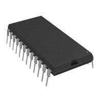
AD1865N-K Analog Devices Inc, AD1865N-K Datasheet - Page 7

AD1865N-K
Manufacturer Part Number
AD1865N-K
Description
IC, DUAL 18-BIT AUDIO DAC
Manufacturer
Analog Devices Inc
Datasheet
1.AD1865N-J.pdf
(12 pages)
Specifications of AD1865N-K
Rohs Status
RoHS non-compliant
Number Of Bits
18
Data Interface
Serial
Number Of Converters
2
Voltage Supply Source
Analog and Digital, Dual ±
Power Dissipation (max)
260mW
Operating Temperature
-25°C ~ 70°C
Mounting Type
Through Hole
Package / Case
24-DIP (0.600", 15.24mm)
Settling Time
-
Lead Free Status / RoHS Status
Available stocks
Company
Part Number
Manufacturer
Quantity
Price
REV. 0
CURRENT OUTPUT MODE
One or both channels of the AD1865 can be operated in current
output mode. I
current-to-voltage (I-V) converter. The internal feedback resis-
tor, R
converter, thus assuring that R
temperature.
Of course, the AD1865 can also be used in voltage output mode
in order to utilize the onboard I-V converter.
INPUT DATA
Data is transmitted to the AD1865 in a bit stream composed of
18-bit words with a serial, twos complement, MSB first format.
Data Left (DL) and Data Right (DR) are the serial inputs for
the left and right DACs, respectively. Similarly, Latch Left (LL)
and Latch Right (LR) update the left and right DACs. The fall-
ing edge of LL and LR cause the last 18 bits which were clocked
into the Serial Registers to be shifted into the DACs, thereby
updating the DAC outputs. Left and Right channels share the
Clock (CLK) signal. Data is clocked into the input registers on
the rising edge of CLK.
Figure 8 illustrates the general signal requirements for data
transfer for the AD1865.
F
, can still be used in the feedback path of the external I-V
OUT
CLK
can be used to directly drive an external
DR
LR
DL
LL
M
M
S
B
S
B
LL/LR
DL/DR
CLK
F
tracks the DAC over time and
>15ns
>15ns
>30ns
>74.1ns
1st BIT
Figure 8. AD1865 Control Signals
MSB
Figure 9. AD1865 Timing Diagram
>30ns
>30ns
UPDATED WITH 18 MOST RECENT BITS
INTERNAL DAC INPUT REGISTER
2nd BIT
–7–
Digital Circuit Considerations–AD1865
TIMING
Figure 9 illustrates the specific timing requirements that must
be met in order for the data transfer to be accomplished prop-
erly. The input pins of the AD1865 are both TTL and 5 V
CMOS compatible.
The minimum clock rate of the AD1865 is at least 13.5 MHz.
This clock rate allows data transfer rates of 2 , 4 , 8 and
16
VOLTAGE OUTPUT MODES
As shown on the block diagram, each channel of the AD1865 is
complete with an I-V converter and a feedback resistor. These
can be connected externally to provide direct voltage output
from one or both AD1865 channels. Figure 6 shows these con-
nections. I
is connected to the feedback resistor, R
results in the lowest possible component count and achieves the
specifications shown on the Specifications page while operating
at 16
F
S
F
(where F
S
.
OUT
18th BIT
LSB
is connected to the Summing Junction, SJ. V
S
>40ns
equals 44.1 kHz).
>40ns
BITS CLOCKED
TO SHIFT REGISTER
>15ns
>40ns
WORD
NEXT
S
B
S
B
L
L
F
. This implementation
OUT


