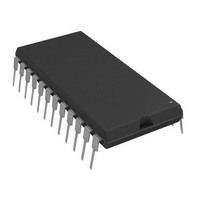
AD1865N-K Analog Devices Inc, AD1865N-K Datasheet - Page 6

AD1865N-K
Manufacturer Part Number
AD1865N-K
Description
IC, DUAL 18-BIT AUDIO DAC
Manufacturer
Analog Devices Inc
Datasheet
1.AD1865N-J.pdf
(12 pages)
Specifications of AD1865N-K
Rohs Status
RoHS non-compliant
Number Of Bits
18
Data Interface
Serial
Number Of Converters
2
Voltage Supply Source
Analog and Digital, Dual ±
Power Dissipation (max)
260mW
Operating Temperature
-25°C ~ 70°C
Mounting Type
Through Hole
Package / Case
24-DIP (0.600", 15.24mm)
Settling Time
-
Lead Free Status / RoHS Status
Available stocks
Company
Part Number
Manufacturer
Quantity
Price
AD1865–Analog Circuit Consideration
GROUNDING RECOMMENDATIONS
The AD1865 has three ground pins, two labeled AGND and
one labeled DGND. AGND, the analog ground pins, are the
“high quality” ground references for the device. To minimize
distortion and reduce crosstalk between channels, the analog
ground pins should be connected together only at the analog
common point in the system. As shown in Figure 6, the AGND
pins should not be connected at the chip.
The digital ground pin returns ground current from the digital
logic portions of the AD1865 circuitry. This pin should be con-
nected to the digital common pin in the system. Other digital
logic chips should also be referred to that point. The analog and
digital grounds should be connected together at one point in the
system, preferably at the power supply.
POWER SUPPLIES AND DECOUPLING
The AD1865 has three power supply input pins. V
the supply voltages which operate the analog portions of the
DAC including the voltage references, output amplifiers and
control amplifiers. The V
from 5 V supplies. Each supply should be decoupled to analog
common using a 0.1 F capacitor in parallel with a 10 F
capacitor. Good engineering practice suggests that the bypass
capacitors be placed as close as possible to the package pins.
This minimizes the parasitic inductive effects of printed circuit
board traces.
The +V
ing the input shift registers and the input latching circuitry.
This supply should be bypassed to digital common using a
0.1 F capacitor in parallel with a 10 F capacitor. +V
ates with a +5 V supply. In order to assure proper operation of
the AD1865, –V
age at all times.
Though separate positive power supply pins are provided for
the analog and digital portions of the AD1865, it is also possible
to use the AD1865 in systems featuring a single +5 V power
supply. In this case, both the +V
connected to the single +5 V power supply. This feature allows
reduction of the cost and complexity of the system power
supply.
L
Figure 6. Recommended Circuit Schematic
–ANALOG
supply operates the digital portions of the chip includ-
SUPPLY
DIGITAL
SUPPLY
V
OUT
S
must be the most negative power supply volt-
10
12
11
1
2
3
4
5
6
7
8
9
NC = NO CONNECT
S
–V
TRIM
MSB
AGND
SJ
DR
CLK
I
R
V
+V
LR
supplies are designed to operate
OUT
F
OUT
S
L
AD1865
S
AGND
DGND
and +V
TRIM
V
MSB
I
+V
OUT
OUT
NC
DL
SJ
R
LL
S
F
24
23
22
20
19
18
17
16
15
14
13
21
L
input pins should be
DIGITAL
COMMON
V
ANALOG
SUPPLY
OUT
S
provides
L
oper-
–6–
As with most linear circuits, changes in the power supplies will
affect the output of the DAC. Analog Devices recommends that
well regulated power supplies with less than 1% ripple be incor-
porated into the design of an audio system.
DISTORTION PERFORMANCE AND TESTING
The THD+N figure of an audio DAC represents the amount of
undesirable signal produced during reconstruction and playback
of an audio waveform. The THD+N specification, therefore,
provides a direct method to classify and choose an audio DAC
for a desired level of performance. Figure 1 illustrates the typ-
ical THD+N performance of the AD1865 versus frequency. A
load impedance of at least 1.5 k is recommended for best
THD+N performance.
Analog Devices tests and grades all AD1865s on the basis of
THD+N performance. During the distortion test, a high-speed
digital pattern generator transmits digital data to each channel
of the device under test. Eighteen-bit data is transmitted at
705.6 kHz (16 F
with 0 dB, –20 dB and –60 dB amplitudes. A 4096 point FFT
calculates total harmonic distortion + noise, signal-to-noise ratio,
D-Range and channel separation. No deglitchers or MSB trims
are used in the testing of the AD1865.
OPTIONAL MSB ADJUSTMENT
Use of optional adjust circuitry allows residual distortion error
to be eliminated. This distortion is especially important when
low amplitude signals are being reproduced. The MSB adjust
circuitry is shown in Figure 7. The trim potentiometer should
be adjusted to produce the lowest distortion using an input sig-
nal with a –60 dB amplitude.
200k
Figure 7. Optional THD+N Adjust Circuitry
100k
S
). The test waveform is a 990.5 Hz sine wave
470k
10
11
12
NC = NO CONNECT
1
2
3
4
5
6
7
8
9
–V
TRIM
MSB
I
AGND
SJ
R
V
+V
DR
LR
CLK
OUT
F
OUT
S
AD1865
L
AGND
DGND
TRIM
V
MSB
I
+V
OUT
OUT
NC
SJ
R
DL
LL
S
F
19
18
16
24
23
22
21
20
17
15
14
13
470k
100k
200k
REV. 0


