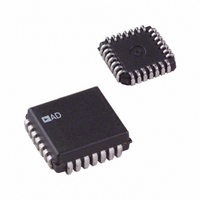
AD1555AP Analog Devices Inc, AD1555AP Datasheet - Page 8

AD1555AP
Manufacturer Part Number
AD1555AP
Description
IC,Converter, Other/Special/Miscellaneous,BICMOS,LDCC,28PIN
Manufacturer
Analog Devices Inc
Datasheet
1.AD1555APZ.pdf
(24 pages)
Specifications of AD1555AP
Rohs Status
RoHS non-compliant
Number Of Bits
24
Sampling Rate (per Second)
256k
Data Interface
Serial, Parallel
Number Of Converters
1
Power Dissipation (max)
96W
Voltage Supply Source
Dual ±
Operating Temperature
0°C ~ 85°C
Mounting Type
Surface Mount
Package / Case
28-LCC (J-Lead)
For Use With
EVAL-AD1555/56EB - BOARD EVAL FOR AD1555/56
Lead Free Status / RoHS Status
Available stocks
Company
Part Number
Manufacturer
Quantity
Price
Part Number:
AD1555AP
Manufacturer:
ADI/亚德诺
Quantity:
20 000
Company:
Part Number:
AD1555APRL
Manufacturer:
Analog Devices Inc
Quantity:
10 000
Company:
Part Number:
AD1555APZ
Manufacturer:
Analog Devices Inc
Quantity:
10 000
Company:
Part Number:
AD1555APZRL
Manufacturer:
Analog Devices Inc
Quantity:
10 000
ABSOLUTE MAXIMUM RATINGS
Analog Inputs
Supply Voltages
Ground Voltage Differences
Digital Inputs . . . . . . . . . . . . . . . . . . . . –0.3 V to V
Internal Power Dissipation
AD1555/AD1556
CAUTION
ESD (electrostatic discharge) sensitive device. Electrostatic charges as high as 4000 V readily
accumulate on the human body and test equipment and can discharge without detection. Although
the AD1555/AD1556 features proprietary ESD protection circuitry, permanent damage may occur
on devices subjected to high energy electrostatic discharges. Therefore, proper ESD precautions are
recommended to avoid performance degradation or loss of functionality.
AIN(+), AIN(–) 2 µs Pulse Input Current . . . . . . . . ± 1.5 A
Pins 7, 8, 23, 24, 25, 28 . . . . . . –V
AIN(+), AIN(–) DC Input Current . . . . . . . . . . . ± 100 mA
+V
+V
–V
V
DGND, AGND1, AGND2, AGND3 . . . . . . . . . . . ± 0.3 V
AD1555 . . . . . . . . . . . . . . . . . . . . . . . . . . . . . . . . . . . 1.8 W
AD1556 . . . . . . . . . . . . . . . . . . . . . . . . . . . . . . . . . . . 1.8 W
L
A
A
A
to DGND . . . . . . . . . . . . . . . . . . . . . . . . –0.3 V to +7 V
to AGND . . . . . . . . . . . . . . . . . . . . . . . –7 V to +0.3 V
to –V
to AGND . . . . . . . . . . . . . . . . . . . . . . . –0.3 V to +7 V
A
Model
AD1555AP
AD1555APRL
AD1555BP
AD1555BPRL
AD1556AS
AD1556ASRL
EVAL-AD1555/AD1556EB
AD1555/56-REF
*Contact factory for extended temperature range.
. . . . . . . . . . . . . . . . . . . . . . . . . –0.3 V to +14 V
2
1
A
– 0.3 V to +V
–55°C to +85 °C
0°C to 85°C
0°C to 85°C
–55°C to +85 °C
–55°C to +85 °C
–55°C to +85 °C
Temperature
Range*
A
L
ORDERING GUIDE
+ 0.3 V
+ 0.3 V
–8–
Plastic Lead Chip Carrier
Plastic Lead Chip Carrier
Plastic Lead Chip Carrier
Plastic Lead Chip Carrier
Plastic Quad Flatpack
Plastic Quad Flatpack
Junction Temperature . . . . . . . . . . . . . . . . . . . . . . . . . 150°C
Storage Temperature . . . . . . . . . . . . . . . . . . –65°C to +150°C
Lead Temperature Range
NOTES
1
2
Package
Description
Stresses above those listed under Absolute Maximum Ratings may cause perma-
Specification is for device in free air:
nent damage to the device. This is a stress rating only; functional operation of the
device at these or any other conditions above those indicated in the operational
section of this specification is not implied. Exposure to absolute maximum rating
conditions for extended periods may affect device reliability.
28-lead PLCC: θ
44-lead MQFP: θ
(Soldering 10 sec) . . . . . . . . . . . . . . . . . . . . . . . . . . 300°C
JA
JA
= 36°C/W, θ
= 36°C/W, θ
JC
JC
= 20°C/W
= 14°C/W
Evaluation Board
Reference Design
P-28A
P-28A
P-28A
P-28A
Package
Option
S-44A
S-44A
WARNING!
ESD SENSITIVE DEVICE
REV. B


