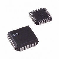
AD1555AP Analog Devices Inc, AD1555AP Datasheet - Page 3

AD1555AP
Manufacturer Part Number
AD1555AP
Description
IC,Converter, Other/Special/Miscellaneous,BICMOS,LDCC,28PIN
Manufacturer
Analog Devices Inc
Datasheet
1.AD1555APZ.pdf
(24 pages)
Specifications of AD1555AP
Rohs Status
RoHS non-compliant
Number Of Bits
24
Sampling Rate (per Second)
256k
Data Interface
Serial, Parallel
Number Of Converters
1
Power Dissipation (max)
96W
Voltage Supply Source
Dual ±
Operating Temperature
0°C ~ 85°C
Mounting Type
Surface Mount
Package / Case
28-LCC (J-Lead)
For Use With
EVAL-AD1555/56EB - BOARD EVAL FOR AD1555/56
Lead Free Status / RoHS Status
Available stocks
Company
Part Number
Manufacturer
Quantity
Price
Part Number:
AD1555AP
Manufacturer:
ADI/亚德诺
Quantity:
20 000
Company:
Part Number:
AD1555APRL
Manufacturer:
Analog Devices Inc
Quantity:
10 000
Company:
Part Number:
AD1555APZ
Manufacturer:
Analog Devices Inc
Quantity:
10 000
Company:
Part Number:
AD1555APZRL
Manufacturer:
Analog Devices Inc
Quantity:
10 000
AD1556–SPECIFICATIONS
Parameter
FILTER PERFORMANCES
DIGITAL INPUTS OUTPUTS
POWER SUPPLIES
TEMPERATURE RANGE
*
Specifications subject to change without notice.
REV. B
Parameter
POWER SUPPLIES
NOTES
10
11
12
Specifications subject to change without notice.
1
2
3
4
5
6
7
8
9
Contact factory for extended temperature range.
Tested at the output word rate F
Tested with a full-scale input signal at approximately 24 Hz.
This parameter is guaranteed by design.
Tested at the output word rate F
This specification is for the AD1555 only and does not include the errors from external components as, for instance, the external reference.
This offset specification is referred to the modulator output.
Characterized with a 100 mV p-p sine wave applied separately to each supply.
Contact factory for extended temperature range.
Recommended Reference: AD780BR.
word rates.
Specified with analog inputs grounded.
See Table III for configuration conditions.
Specified with MCLK input grounded.
Pass-Band Ripple
Stop-Band Attenuation
Filters Characteristics
V
V
I
I
V
V
Specified Performance
Quiescent Currents
Power Dissipation
Specified Performance, T
Recommended Operating Conditions
Quiescent Currents
Power Dissipation
IL
IH
IL
IH
OL
OH
V
I(V
+V
–V
V
I(+V
I(–V
I(V
L
L
A
A
L
L
)
)
A
A
)
)
10
10
10
*
MIN
O
O
= 1 kHz. F
= 1 kHz with input signals of 30 Hz and 50 Hz, each 6 dB down full scale.
to T
MAX
Notes
PGA in Standby Mode
In Power-Down Mode
Reference Input = 3 V
Reference Input = 0 V
O
is the AD1556 output word rate, the inverse of the sampling rate. See Tables I, Ia, Ib for other output
Notes
All Filters Except F
F
I
I
V
In Power-Down Mode
SINK
SOURCE
O
L
= 3.3 V, F
=16 kHz
(V
= +2 mA
L
= –2 mA
= 2.85 V to 5.25 V; CLKIN = 1.024 MHz; T
11, 12
11
O
= 1 kHz
–3–
O
=16 kHz
Min
4.75
–5.25
4.75
AD1555BP
Typ
5
–5
5
8
8
30
77
56
650
250
Min
–0.05
–0.3
+2.0
–10
–10
V
2.85
–55
L
Max
5.25
–4.75
5.25
10
9.5
42
96
70
– 0.6
AD1556AS
See Table II
A
= T
Min
4.75
–5.25
4.75
MIN
Typ
4
6.2
70
to T
AD1555AP
MAX
Typ
5
–5
5
8
8
30
77
56
650
250
unless otherwise noted.)
AD1555/AD1556
Max
+0.05
–135
–86
+0.8
V
+10
+10
+0.5
5.25
5
8.5
+85
L
Max
5.25
–4.75
5.25
10
9.5
42
96
70
+ 0.3
Unit
dB
dB
dB
V
V
µA
µA
V
V
V
mA
mW
µW
°C
Unit
V
V
V
mA
mA
µA
mW
mW
µW
µW


