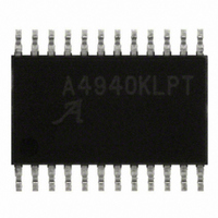
A4940KLPTR-T Allegro Microsystems Inc, A4940KLPTR-T Datasheet - Page 6

A4940KLPTR-T
Manufacturer Part Number
A4940KLPTR-T
Description
FULL BRIDGE MOSFET PRE-DRIVER
Manufacturer
Allegro Microsystems Inc
Datasheet
1.A4940KLPTR-T.pdf
(14 pages)
Specifications of A4940KLPTR-T
Configuration
H Bridge
Input Type
Non-Inverting
Delay Time
35ns
Number Of Configurations
1
Number Of Outputs
4
Voltage - Supply
5.5 V ~ 50 V
Operating Temperature
-40°C ~ 150°C
Mounting Type
Surface Mount
Package / Case
24-TSSOP Exposed Pad, 24-eTSSOP, 24-HTSSOP
Lead Free Status / RoHS Status
Lead free / RoHS Compliant
Current - Peak
-
High Side Voltage - Max (bootstrap)
-
Lead Free Status / RoHS Status
Lead free / RoHS Compliant
Other names
620-1319-2
Available stocks
Company
Part Number
Manufacturer
Quantity
Price
Company:
Part Number:
A4940KLPTR-T
Manufacturer:
ALLEGRO
Quantity:
356
Part Number:
A4940KLPTR-T
Manufacturer:
ALLEGRO/雅丽高
Quantity:
20 000
A4940
The A4940 is a full-bridge MOSFET driver (pre-driver) requir-
ing an unregulated supply of 7 to 50 V and a logic supply from
3 to 5.5 V.
The four gate drives are capable of driving a wide range of
N-channel power MOSFETs, and are configured as two high-
side drives and two low-side drives. The A4940 provides all the
necessary circuits to ensure that the gate-source voltage of both
high-side and low-side external MOSFETs are above 10 V, at
supply voltages down to 7 V. For extreme battery voltage drop
conditions, correct functional operation is guaranteed at supply
voltages down to 5.5 V, but with a reduced gate drive voltage.
The A4940 provides the interface between the logic level outputs
of a microcontroller and the high current, high voltage gate drive
for N-channel power MOSFETs in a full-bridge configuration.
Typically, the power full-bridge will be used for brush DC motor
control or other high current inductor loads. Each MOSFET in
the bridge is controlled by an independent logic level input com-
patible with 3.3 or 5 V logic outputs. Cross-conduction (shoot-
through) in the external bridge is avoided by an adjustable dead
time.
A low power sleep mode allows the A4940, the power bridge, and
the load to remain connected to a vehicle battery supply without
the need for an additional supply switch.
The A4940 provides a single fault flag to indicate undervoltage
and overtemperature conditions.
Power Supplies
Two power supply connections are required, one for the logic
interface, and one for the analog and output drive sections.
The logic supply, connected to VDD, allows the flexibility of a
3.3 or 5 V logic interface. The main power supply should be con-
nected to VBB through a reverse voltage protection circuit. Both
supplies should be decoupled with ceramic capacitors connected
close to the supply and ground pins.
The A4940 operates within specified parameters with a VBB
supply from 7 to 50 V and will function correctly with a supply
down to 5.5 V. This provides a very rugged solution for use in the
harsh automotive environment.
Gate Drives
The A4940 is designed to drive external, low on-resistance,
power N-channel MOSFETs. It supplies the large transient
Functional Description
Automotive Full Bridge MOSFET Driver
currents necessary to quickly charge and discharge the external
MOSFET gate capacitance in order to reduce dissipation in the
MOSFET during switching. The charge and discharge rate can be
controlled using an external resistor in series with the connection
to the gate of the MOSFET.
Gate Drive Voltage Regulation The gate drives are powered
by an internal regulator, which limits the supply to the drives and
therefore the maximum gate voltage. When the VBB supply is
greater than about 16 V, the regulator is a simple linear regulator.
Below 16 V, the regulated supply is maintained by a charge pump
boost converter, which requires a pump capacitor connected
between the CP1 and CP2 pins. This capacitor must have a mini-
mum value of 220 nF, and is typically 470 nF.
The regulated voltage, 13 V typical, is available on the VREG
pin. A sufficiently large storage capacitor must be connected to
this pin to provide the transient charging current to the low-side
drives and the bootstrap capacitors.
GLA and GLB Pins These are the low-side gate drive outputs
for the external N-channel MOSFETs. External resistors between
the gate drive output and the gate connection to the MOSFET (as
close as possible to the MOSFET) can be used to control the slew
rate seen at the gate, thereby providing some control of the di/dt
and dv/dt of the SA and SB outputs. GLx going high turns on the
upper half of the drive, sourcing current to the gate of the low-
side MOSFET in the external power bridge, turning it on. GLx
going low turns on the lower half of the drive, sinking current
from the external MOSFET gate circuit to GND pin, turning off
the MOSFET.
SA and SB Pins Directly connected to the motor, these termi-
nals sense the voltages switched across the load. These terminals
are also connected to the negative side of the bootstrap capacitors
and are the negative supply connections for the floating high-side
drives. The discharge current from the high-side MOSFET gate
capacitance flows through these connections, which should have
low impedance circuit connections to the MOSFET bridge.
GHA and GHB Pins These terminals are the high-side gate
drive outputs for the external N-channel MOSFETs. External
resistors between the gate drive output and the gate connection to
the MOSFET (as close as possible to the MOSFET) can be used
to control the slew rate seen at the gate, thereby controlling the
di/dt and dv/dt of the SA and SB outputs. GHx going high turns
115 Northeast Cutoff
1.508.853.5000; www.allegromicro.com
Allegro MicroSystems, Inc.
Worcester, Massachusetts 01615-0036 U.S.A.
6


