74LVCH322244AEC;55 NXP Semiconductors, 74LVCH322244AEC;55 Datasheet - Page 2
74LVCH322244AEC;55
Manufacturer Part Number
74LVCH322244AEC;55
Description
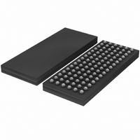
74LVCH322244AEC/LFBGA96/TRAYDP
Manufacturer
NXP Semiconductors
Series
74LVCHr
Datasheet
1.74LVCH322244AEC51.pdf
(12 pages)
Specifications of 74LVCH322244AEC;55
Logic Type
Buffer/Line Driver, Non-Inverting
Number Of Elements
8
Number Of Bits Per Element
4
Current - Output High, Low
12mA, 12mA
Voltage - Supply
1.2 V ~ 3.6 V
Operating Temperature
-40°C ~ 85°C
Mounting Type
Surface Mount
Package / Case
96-LFBGA
Logic Family
LVC
Number Of Channels Per Chip
32
Polarity
Non-Inverting
Supply Voltage (max)
3.6 V
Supply Voltage (min)
1.2 V
Maximum Operating Temperature
+ 85 C
Mounting Style
SMD/SMT
High Level Output Current
- 12 mA
Low Level Output Current
12 mA
Minimum Operating Temperature
- 40 C
Number Of Lines (input / Output)
32 / 32
Output Type
3-State
Propagation Delay Time
11 ns at 1.2 V, 3 ns at 3.3 V
Lead Free Status / RoHS Status
Lead free / RoHS Compliant
Lead Free Status / RoHS Status
Lead free / RoHS Compliant
Other names
74LVCH322244AEC
74LVCH322244AEC
935263930557
74LVCH322244AEC
935263930557


Philips Semiconductors
FEATURES
QUICK REFERENCE DATA
Ground = 0 V; T
Notes
1. C
2. The condition is V
2004 May 25
t
t
t
C
C
PHL
PZH
PHZ
SYMBOL
5 V tolerant inputs/outputs for interfacing with 5 V logic
Wide supply voltage range from 1.2 V to 3.6 V
CMOS low power consumption
MULTIBYTE flow-trough standard pin-out architecture
Low inductance multiple power and ground pins for
minimum noise and ground bounce
Direct interface with TTL levels
Inputs accept voltages up to 5.5 V
All data inputs have bushold
Integrated 30
Complies with JEDEC standard JESD8B/JESD36
ESD protection:
HBM EIA/JESD22-A114-B exceeds 2000 V
MM EIA/JESD22-A115-A exceeds 200 V.
Specified from 40 C to +85 C
Packaged in plastic fine-pitch ball grid array package.
I
PD
32-bit buffer/line driver; with 30
resistors; 5 V input/output tolerant; 3-state
P
f
f
C
V
N = total load switching outputs;
i
o
/t
/t
/t
(C
D
CC
PD
= input frequency in MHz;
L
PLH
PZL
PLZ
= output frequency in MHz;
= output load capacitance in pF;
= C
L
is used to determine the dynamic power dissipation (P
= supply voltage in Volts;
PD
V
CC
propagation delay nAn to nYn
3-state output enable time nOE to nYn
3-state output disable time nOE to nYn
input capacitance
power dissipation capacitance per gate
2
V
amb
CC
termination resistors
f
o
2
= 25 C; t
) = sum of the outputs.
I
f
= GND to V
i
N + (C
PARAMETER
r
= t
f
L
CC
2.5 ns.
.
V
CC
2
f
o
) where:
series termination
2
C
C
C
V
DESCRIPTION
The 74LVCH322244A is a high-performance, low-power,
low-voltage, Si-gate CMOS device, superior to most
advanced CMOS compatible TTL families. Inputs can be
driven from either 3.3 V or 5 V devices. In 3-state
operation, outputs can handle 5 V. These features allow
the use of these devices in a mixed 3.3 V and 5 V
environment.
The 74LVCH322244A is a 32-bit non-inverting buffer/line
driver with 3-state outputs. The 3-state outputs are
controlled by the output enable inputs nOE. A HIGH on
input nOE causes the outputs to assume a
high-impedance OFF-state.
The 74LVCH322244A is designed with 30
termination resistors in both HIGH and LOW output stages
to reduce line noise.
To ensure the high-impedance state during power-up or
power-down, input nOE should be tied to V
pull-up resistor; the minimum value of the resistor is
determined by the current-sinking capability of the driver.
The 74LVCH322244A bushold data input circuit eliminates
the need for external pull-up resistors to hold unused or
floating data inputs at a valid logic level.
I
L
L
L
outputs enabled
outputs disabled
D
= 3.3 V; notes 1 and 2
= 50 pF; V
= 50 pF; V
= 50 pF; V
in W).
CONDITIONS
CC
CC
CC
= 3.3 V
= 3.3 V
= 3.3 V
3.0
3.5
2.8
5.0
12
4.0
74LVCH322244A
TYPICAL
Product specification
CC
ns
ns
ns
pF
pF
pF
series
through a
UNIT
Related parts for 74LVCH322244AEC;55
Image
Part Number
Description
Manufacturer
Datasheet
Request
R

Part Number:
Description:
NXP Semiconductors designed the LPC2420/2460 microcontroller around a 16-bit/32-bitARM7TDMI-S CPU core with real-time debug interfaces that include both JTAG andembedded trace
Manufacturer:
NXP Semiconductors
Datasheet:

Part Number:
Description:
NXP Semiconductors designed the LPC2458 microcontroller around a 16-bit/32-bitARM7TDMI-S CPU core with real-time debug interfaces that include both JTAG andembedded trace
Manufacturer:
NXP Semiconductors
Datasheet:
Part Number:
Description:
NXP Semiconductors designed the LPC2468 microcontroller around a 16-bit/32-bitARM7TDMI-S CPU core with real-time debug interfaces that include both JTAG andembedded trace
Manufacturer:
NXP Semiconductors
Datasheet:
Part Number:
Description:
NXP Semiconductors designed the LPC2470 microcontroller, powered by theARM7TDMI-S core, to be a highly integrated microcontroller for a wide range ofapplications that require advanced communications and high quality graphic displays
Manufacturer:
NXP Semiconductors
Datasheet:
Part Number:
Description:
NXP Semiconductors designed the LPC2478 microcontroller, powered by theARM7TDMI-S core, to be a highly integrated microcontroller for a wide range ofapplications that require advanced communications and high quality graphic displays
Manufacturer:
NXP Semiconductors
Datasheet:
Part Number:
Description:
The Philips Semiconductors XA (eXtended Architecture) family of 16-bit single-chip microcontrollers is powerful enough to easily handle the requirements of high performance embedded applications, yet inexpensive enough to compete in the market for hi
Manufacturer:
NXP Semiconductors
Datasheet:
Part Number:
Description:
The XA-S3 device is a member of Philips Semiconductors? XA(eXtended Architecture) family of high performance 16-bitsingle-chip microcontrollers
Manufacturer:
NXP Semiconductors
Datasheet:

Part Number:
Description:
The NXP BlueStreak LH75401/LH75411 family consists of two low-cost 16/32-bit System-on-Chip (SoC) devices
Manufacturer:
NXP Semiconductors
Datasheet:
Part Number:
Description:
The NXP LPC3130/3131 combine an 180 MHz ARM926EJ-S CPU core, high-speed USB2
Manufacturer:
NXP Semiconductors
Datasheet:
Part Number:
Description:
The NXP LPC3141 combine a 270 MHz ARM926EJ-S CPU core, High-speed USB 2
Manufacturer:
NXP Semiconductors
Part Number:
Description:
The NXP LPC3143 combine a 270 MHz ARM926EJ-S CPU core, High-speed USB 2
Manufacturer:
NXP Semiconductors

Part Number:
Description:
The NXP LPC3152 combines an 180 MHz ARM926EJ-S CPU core, High-speed USB 2
Manufacturer:
NXP Semiconductors
Part Number:
Description:
The NXP LPC3154 combines an 180 MHz ARM926EJ-S CPU core, High-speed USB 2
Manufacturer:
NXP Semiconductors

Part Number:
Description:
Standard level N-channel enhancement mode Field-Effect Transistor (FET) in a plastic package using NXP High-Performance Automotive (HPA) TrenchMOS technology
Manufacturer:
NXP Semiconductors
Datasheet: