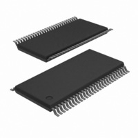
74ALVCH16600DGG:11 NXP Semiconductors, 74ALVCH16600DGG:11 Datasheet - Page 2

74ALVCH16600DGG:11
Manufacturer Part Number
74ALVCH16600DGG:11
Description
74ALVCH16600DGG/TSSOP56/REEL13
Manufacturer
NXP Semiconductors
Series
74ALVCHr
Datasheet
1.74ALVCH16600DGG11.pdf
(14 pages)
Specifications of 74ALVCH16600DGG:11
Logic Type
Universal Bus Transceiver
Number Of Circuits
18-Bit
Current - Output High, Low
24mA, 24mA
Voltage - Supply
2.3 V ~ 3.6 V
Operating Temperature
-40°C ~ 85°C
Mounting Type
Surface Mount
Package / Case
56-TSSOP
Lead Free Status / RoHS Status
Lead free / RoHS Compliant
Other names
74ALVCH16600DG-T
74ALVCH16600DG-T
935262545118
74ALVCH16600DG-T
935262545118
1.
Philips Semiconductors
FEATURES
QUICK REFERENCE DATA
GND = 0V; T
NOTES:
ORDERING INFORMATION
56-Pin Plastic TSSOP Type II
1998 Sep 24
Complies with JEDEC standard no. 8-1A.
CMOS low power consumption
Direct interface with TTL levels
Current drive
All inputs have bus hold circuitry
Output drive capability 50 transmission lines @ 85 C
MULTIBYTE
Low inductance multiple V
and ground bounce
18-bit universal bus transceiver (3-State)
t
C
C
C
C
PHL
SYMBOL
I/O
I
PD
C
P
f
f
S (C
i
o
D
PD
= input frequency in MHz; C
/t
= output frequency in MHz; V
PLH
= C
L
is used to determine the dynamic power dissipation (P
PD
amb
V
CC
TM
PACKAGES
= 25 C; t
V
2
24 mA at 3.0 V
flow-through standard pin-out architecture
Propagation delay
An, Bn to Bn, An
Input/Output capacitance
Input capacitance
Power dissipation capacitance per latch
Power dissipation capacitance per latch
CC
f
2
o
) = sum of outputs.
f
i
r
+ S (C
= t
CC
f
= 2.5ns
and ground pins for minimum noise
L
PARAMETER
L
= output load capacitance in pF;
V
CC
CC
= supply voltage in V;
2
f
o
) where:
TEMPERATURE RANGE
–40 C to +85 C
D
V
V
V = GND to V
V
in mW):
CC
CC
I
= GND to V
= 2.5V, C
= 3.3V, C
2
DESCRIPTION
The 74ALVCH16600 is an 18-bit universal transceiver featuring
non-inverting 3-State bus compatible outputs in both send and
receive directions. Data flow in each direction is controlled by output
enable (OE
(CP
in the transparent mode when LE
A data is latched if CP
is Low, the A-bus data is stored in the latch/flip-flop on the
High-to-Low transition of CP
active. When OE
state. The High clock can be controlled with the clock-enable inputs
(CE
Data flow for B-to-A is similar to that of A-to-B but uses OE
and CP
To ensure the high impedance state during power up or power
down, OE
resistor; the minimum value of the resistor is determined by the
current-sinking/current-sourcing capability of the driver.
Active bus hold circuitry is provided to hold unused or floating data
inputs at a valid logic level.
AB
BA
L
L
CC
CC
= 30pF
= 50pF
/CE
and CP
1
1
BA
CONDITIONS
OUTSIDE NORTH AMERICA
.
BA
AB
AB
).
and OE
74ALVCH16600 DGG
BA
and OE
) inputs. For A-to-B data flow, the device operates
AB
Outputs enabled
Outputs disabled
is High, the outputs are in the high-impedance
AB
AB
BA
should be tied to V
), latch enable (LE
is held at a High or Low logic level. If LE
AB
. When OE
AB
is High. When LE
74ALVCH16600
AB
CC
TYPICAL
AB
is Low, the outputs are
through a pullup
Product specification
and LE
3.1
2.8
8.0
4.0
21
3
DWG NUMBER
SOT364-1
853-2123 20077
BA
AB
), and clock
is Low, the
UNIT
BA
pF
pF
pF
pF
ns
, LE
BA
AB


