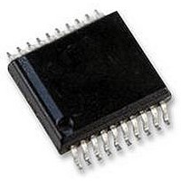
TDA8547TS/N1 NXP Semiconductors, TDA8547TS/N1 Datasheet - Page 5

TDA8547TS/N1
Manufacturer Part Number
TDA8547TS/N1
Description
AMP, AUDIO, PWR, 1.2W, AB, 20SSOP
Manufacturer
NXP Semiconductors
Datasheet
1.TDA8547TSN1.pdf
(20 pages)
Specifications of TDA8547TS/N1
Amplifier Class
AB
No. Of Channels
2
Output Power
1.2W
Load Impedance
16ohm
Operating Temperature Range
-40°C To +85°C
Amplifier Case Style
SSOP
No. Of Pins
20
Base Number
8547
Supply Voltage Range
2.2V To 18V
Thd + N
0.15% @ 0.4W, 8ohm, VCC=5V
Rohs Compliant
Yes
Lead Free Status / RoHS Status
Lead free / RoHS Compliant
Available stocks
Company
Part Number
Manufacturer
Quantity
Price
Company:
Part Number:
TDA8547TS/N1
Manufacturer:
NXP
Quantity:
1 000
Company:
Part Number:
TDA8547TS/N1Ј¬118
Manufacturer:
NXP
Quantity:
10 000
Philips Semiconductors
SELECT pin
If the voltage at the SELECT pin is in the range between
1.5 V and V
channels can be operational. If the SELECT pin is set to a
LOW voltage or grounded, then only channel 2 can
operate and the power amplifier of channel 1 will be in the
standby mode. In this case only the loudspeaker at
channel 2 can operate and the loudspeaker at channel 1
will be switched off. If the SELECT pin is set to a
HIGH level or connected to V
operate and the power amplifier of channel 2 will be in the
standby mode. In this case only the loudspeaker at
channel 1 can operate and the loudspeaker at channel 2
will be switched off. Setting the SELECT pin to a LOW or
Table 1 Control pins MODE and SELECT versus status of output channels
Voltage levels at control pins at V
Notes
1. HIGH = V
2. NC = not connected or floating.
3. X = don’t care.
4. HVP = 1.5 V < V
5. LOW = V
LIMITING VALUES
In accordance with the Absolute Maximum Rating System (IEC 134).
1998 Apr 01
V
V
I
T
T
V
P
ORM
SYMBOL
stg
amb
CC
I
Psc
tot
2
output channel switching
0.7 W BTL audio amplifier with
HVP
HVP
HVP
CC
HIGH
pin
supply voltage
input voltage
repetitive peak output current
storage temperature
operating ambient temperature
AC and DC short-circuit safe voltage
power dissipation
pin
LOW
MODE
HVP
(4)
(4)
(4)
< 0.5 V.
> V
1.5 V, or if it is kept floating, then both
(1)
/LOW
/LOW
/LOW
/NC
(4)
CC
(5)
pin
(2)
< V
(5)
(5)
(5)
0.5 V.
PARAMETER
CC
CC
CONTROL PIN
, then only channel 1 can
1.5 V.
P
= 5 V; for other supply voltages see Figs. 14 and 15.
HVP
HVP
HVP
SELECT
HIGH
LOW
operating
X
(4)
(4)
(4)
(3)
/NC
/NC
/NC
CONDITIONS
(5)
(1)
5
(2)
(2)
(2)
a HIGH voltage results in a reduction of quiescent current
consumption by a factor of approximately 2.
Switching with the SELECT pin during operating is not
plop-free, because the input capacitor of the channel
which is coming out of standby needs to be charged first.
For plop-free channel selecting the device has first to be
set in mute condition with the MODE pin (between 1.5 V
and V
level, after a delay set the MODE pin to a LOW level.
The delay needed depends on the values of the input
capacitor and the feedback resistors. Time needed is
approx. 10
the values in Fig.4.
CC
1.5 V), then set the SELECT pin to the new
C1
CHANNEL 1 CHANNEL 2
0.3
0.3
55
40
mute/on
mute/on
STATUS OF OUTPUT
standby
standby
mute
(R1 + R2), so approximately 0.6 s. for
MIN.
on
CHANNEL
+18
V
1
+150
+85
10
1.1
CC
mute/on
mute/on
standby
standby
MAX.
mute
+ 0.3
on
TDA8547TS
Product specification
V
V
A
V
W
C
C
TYP. I
(mA)
UNIT
15
15
15
0
8
8
q


