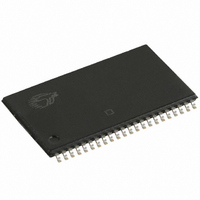
CY7C1021D-10ZSXIT Cypress Semiconductor Corp, CY7C1021D-10ZSXIT Datasheet

CY7C1021D-10ZSXIT
Specifications of CY7C1021D-10ZSXIT
Related parts for CY7C1021D-10ZSXIT
CY7C1021D-10ZSXIT Summary of contents
Page 1
... Document #: 38-05462 Rev. *J 1-Mbit (64 K × 16) Static RAM Functional Description The CY7C1021D is a high performance CMOS static RAM organized as 65,536 words by 16 bits. This device has an automatic power down feature that significantly reduces power consumption when deselected. The input and output pins (IO ...
Page 2
... Data Retention Waveform ................................................ 7 Switching Waveforms ...................................................... 7 Truth Table ...................................................................... 10 Document #: 38-05462 Rev. *J Ordering Information ...................................................... 11 Ordering Code Definitions ......................................... 11 Package Diagrams .......................................................... 12 Acronyms ........................................................................ 14 Document Conventions ................................................. 14 Units of Measure ....................................................... 14 Document History Page ................................................. 15 Sales, Solutions, and Legal Information ...................... 16 Worldwide Sales and Design Support ....................... 16 Products .................................................................... 16 PSoC Solutions ......................................................... 16 CY7C1021D Page [+] Feedback ...
Page 3
... Pin Configuration Figure 1. 44-pin SOJ / 44-pin TSOP II (Top View) Selection Guide Maximum Access Time Maximum Operating Current Maximum CMOS Standby Current Note 1. NC pins are not connected on the die. Document #: 38-05462 Rev BHE BLE Description CY7C1021D [1] -10 (Industrial) Unit Page [+] Feedback ...
Page 4
... Output Disabled Max mA, 100 MHz CC OUT 1/t max RC 83 MHz 66 MHz 40 MHz Max > > < Max > V – 0 > V – 0 < 0 CY7C1021D + 0 Speed 10 -10 (Industrial) Unit Min Max 2.4 – V – 0 0.5 0.8 V 1 A +1 1 A +1 – – – – ...
Page 5
... Rise Time: High-Z characteristics: R1 480 OUTPUT 255 INCLUDING JIG AND SCOPE (c) Figure 2 (a). High Z characteristics are tested for all speeds using the test load CY7C1021D Max Unit 44-pin SOJ 44-pin TSOP II Unit C/W 59.52 53.91 C/W 36.75 21 ...
Page 6
... The input data setup and hold timing should be referenced to the leading edge of the signal that terminates the write. Document #: 38-05462 Rev. *J Description values until the first memory access can be performed less than less than t , and t HZCE LZCE HZOE LZOE HZWE Figure 2 on page CY7C1021D -10 (Industrial) Min Max 100 – 10 – – – – 10 – – ...
Page 7
... WE is HIGH for read cycle. Document #: 38-05462 Rev. *J Conditions 2 > > V – 0 < 0 DATA RETENTION MODE 4.5 V > CDR OHA > 50 s or stable at V > 50 CC(min) CC(min CY7C1021D Min Max Unit 2.0 – V – 0.3 V, – – – 4 [12, 13] DATA VALID Page [+] Feedback ...
Page 8
... OE t DOE t LZOE BHE, BLE t DBE t LZBE HIGH IMPEDANCE DATA OUT t LZCE SUPPLY CURRENT Notes 14 HIGH for read cycle. 15. Address valid prior to or coincident with CE transition LOW. Document #: 38-05462 Rev DATA VALID 50% CY7C1021D [14, 15] t HZOE t HZCE t HZBE HIGH IMPEDANCE 50 Page [+] Feedback ...
Page 9
... Figure 6. Write Cycle No. 2 (BLE or BHE Controlled) ADDRESS t SA BHE, BLE WE CE DATA I/O Notes 16. Data I/O is high impedance BHE and/or BLE = V 17 goes HIGH simultaneously with WE going HIGH, the output remains in a high impedance state. Document #: 38-05462 Rev. *J [16, 17 SCE PWE PWE t SCE CY7C1021D Page [+] Feedback ...
Page 10
... Read – Upper bits only Data In Data In Write – All bits Data In High Z Write – Lower bits only High Z Data In Write – Upper bits only High Z High Z Selected, Outputs Disabled High Z High Z Selected, Outputs Disabled CY7C1021D LZWE Mode Power Standby ( Active ( Active (I ...
Page 11
... TSOP Type II (Pb-free Temperature Range Industrial Pb-free Package Type 44-pin Molded SOJ ZS = 44-pin TSOP Type II Speed C9 Technology 1 = Data width × 16-bits 02 = 1-Mbit density 1 = Fast Asynchronous SRAM family Technology Code CMOS Marketing Code SRAM Company ID Cypress CY7C1021D Operating Range Industrial Page [+] Feedback ...
Page 12
... Package Diagrams Figure 8. 44-pin Molded SOJ (400-Mil) V44.4, 51-85082 Document #: 38-05462 Rev. *J CY7C1021D 51-85082 *C Page [+] Feedback ...
Page 13
... Package Diagrams (continued) Document #: 38-05462 Rev. *J Figure 9. 44-pin TSOP Z44-II, 51-85087 CY7C1021D 51-85087 *C Page [+] Feedback ...
Page 14
... Document #: 38-05462 Rev. *J Document Conventions Units of Measure Symbol Unit of Measure °C degree Celsius MHz Mega Hertz µA micro Amperes µs micro seconds mA milli Amperes mm milli meter ms milli seconds ns nano seconds ohms % percent pF pico Farad V Volts W Watts % percent CY7C1021D Page [+] Feedback ...
Page 15
... Document History Page Document Title: CY7C1021D, 1-Mbit (64 K × 16) Static RAM Document Number: 38-05462 Orig. of Submission Rev. ECN No. Change ** 201560 SWI See ECN *A 233695 RKF See ECN *B 263769 RKF See ECN *C 307601 RKF See ECN *D 520647 VKN See ECN *E 802877 VKN ...
Page 16
... Cypress against all charges. Use may be limited by and subject to the applicable Cypress software license agreement. Document #: 38-05462 Rev. *J All products and company names mentioned in this document may be the trademarks of their respective holders. cypress.com/go/plc Revised June 7, 2011 CY7C1021D PSoC Solutions psoc.cypress.com/solutions PSoC 1 | PSoC 3 ...


