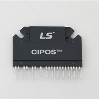
IKCS12F60AA Infineon Technologies, IKCS12F60AA Datasheet - Page 7

IKCS12F60AA
Manufacturer Part Number
IKCS12F60AA
Description
IGBT Modules CiPoS Single In-Line 600V 12A
Manufacturer
Infineon Technologies
Datasheet
1.IKCS12F60AA.pdf
(17 pages)
Specifications of IKCS12F60AA
Collector-emitter Saturation Voltage
2.1 V
Power Dissipation
35 W
Maximum Operating Temperature
+ 125 C
Mounting Style
Through Hole
Package / Case
MSIP-20
Lead Free Status / RoHS Status
Lead free / RoHS Compliant
Available stocks
Company
Part Number
Manufacturer
Quantity
Price
A minimum deadtime insertion of typ 325ns is also
provided, in order to reduce cross-conduction of
the external power switches.
EN (enable, Pin 24)
The signal applied to pin EN controls directly the
output stages. All outputs are set to LOW, if EN is
at LOW logic level. The internal structure of the
pin is the same as Figure 1 made exception of the
switching levels of the Schmitt-Trigger, which are
here V
typical propagation delay time is t
This pin may also be used for reading out the
temperature close to the gate drive IC. Please
refer to section “Integrated Components” for the
specification of the integrated parts.
ITRIP (Over-current detection function, Pin 21)
CiPoS™ provides an over-current detection
function by connecting the ITRIP input with the
motor current feedback. The ITRIP comparator
threshold (typ 0.45V) is referenced to VSS
ground. A input noise filter (typ: t
prevents the driver to detect false over-current
events.
Over-current detection generates a hard shut
down of all outputs of the gate driver after the
shutdown propagation delay of typically 690ns.
The fault-clear time is set to typically to 2ms.
VDD, VSS (control side supply and reference,
Pin 22, 23)
VDD is the low side supply and it provides power
both to input logic and to low side output power
stage. Input logic is referenced to VSS ground as
well as the under-voltage detection circuit.
The under-voltage circuit enables the device to
operate at power on when a supply voltage of at
least a typical voltage of V
least present.
Preliminary Data Sheet
Figure 3: Internal Circuit at pin EN
EN,TH+
= 2.1 V and V
DDUV+
EN,TH-
EN
ITRIPMIN
= 11.9 V is at
= 1.32 V. The
= 700 ns.
= 225ns)
7/17
The IC shuts down all the gate drivers power
outputs, when the VCC supply voltage is below
V
switches from critically low gate voltage levels
during on-state and therefore from excessive
power dissipation.
VB1,2,3 and VS1,2,3 (High side supplies, Pin 1,
2, 4, 5, 7, 8)
VB to VS is the high side supply voltage. The high
side circuit can float with respect to VSS following
the
emitter/source voltage.
Due to the low power consumption, the floating
driver stage is supplied by an integrated bootstrap
circuit connected to VDD. This includes also
integrated bootstrap capacitors of 100 nF at each
floating supply, which are located very close to the
gate drive circuit.
The under-voltage detection operates with a rising
supply threshold of typical V
falling threshold of V
Figure 4.
VS1,2,3 provide a high robustness against
negative voltage in respect of VSS of -50 V. This
ensures very stable designs even under rough
conditions.
VRU, VRV, VRW (low side emitter, Pin 12, 13,
14)
The low side emitters are available for current
measurements
recommended to keep the connection to pin VSS
as short as possible in order to avoid unnecessary
inductive voltage drops.
V+ (positive bus input voltage, Pin 10)
The high side IGBT are connected to the bus
voltage. It is recommended, that the bus voltage
does not exceed 500 V.
Figure 4: Input filter timing diagram
DDUV-
external
= 10.3 V. This prevents the external power
of
high
CIPOS™ IKCS12F60AA
DDUV-
each
side
= 10.3 V according to
BSUV+
phase
Rev. 1.4, Dec. 2007
power
= 11.9 V and a
leg.
device
It
is


