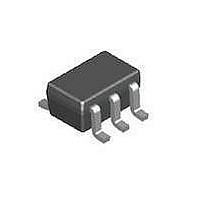
NSBC123JPDXV6T5 ON Semiconductor, NSBC123JPDXV6T5 Datasheet - Page 2

NSBC123JPDXV6T5
Manufacturer Part Number
NSBC123JPDXV6T5
Description
Digital Transistors 100mA Complementary
Manufacturer
ON Semiconductor
Datasheet
1.NSBC124XPDXV6T5.pdf
(14 pages)
Specifications of NSBC123JPDXV6T5
Configuration
Dual
Transistor Polarity
PNP
Typical Input Resistor
2.2 KOhms
Typical Resistor Ratio
0.047
Mounting Style
SMD/SMT
Package / Case
SOT-563-6
Collector- Emitter Voltage Vceo Max
50 V
Continuous Collector Current
0.1 A
Peak Dc Collector Current
100 mA
Power Dissipation
357 mW
Maximum Operating Temperature
+ 150 C
Minimum Operating Temperature
- 55 C
Lead Free Status / RoHS Status
Lead free / RoHS Compliant
Available stocks
Company
Part Number
Manufacturer
Quantity
Price
Company:
Part Number:
NSBC123JPDXV6T5G
Manufacturer:
ON Semiconductor
Quantity:
12 500
DEVICE MARKING AND RESISTOR VALUES
ELECTRICAL CHARACTERISTICS
(T
OFF CHARACTERISTICS
ON CHARACTERISTICS (Note 3)
2. New resistor combinations. Updated curves to follow in subsequent data sheets.
3. Pulse Test: Pulse Width < 300 ms, Duty Cycle < 2.0%
NSBC114EPDXV6T1G
NSBC124EPDXV6T1G
NSBC144EPDXV6T1G
NSBC114YPDXV6T1G
NSBC114TPDXV6T1G (Note 2)
NSBC143TPDXV6T1G (Note 2)
NSBC113EPDXV6T1G (Note 2)
NSBC123EPDXV6T1G (Note 2)
NSBC143EPDXV6T1G (Note 2)
NSBC143ZPDXV6T1G (Note 2)
NSBC124XPDXV6T1G (Note 2)
NSBC123JPDXV6T1G (Note 2)
Collector-Base Cutoff Current (V
Collector-Emitter Cutoff Current (V
Emitter-Base Cutoff Current
(V
Collector-Base Breakdown Voltage (I
Collector-Emitter Breakdown Voltage (Note 3) (I
DC Current Gain
(V
A
EB
CE
= 25°C unless otherwise noted, common for Q
= 6.0 V, I
= 10 V, I
C
C
= 5.0 mA)
= 0)
Device
Characteristic
CB
CE
= 50 V, I
C
= 50 V, I
= 10 mA, I
E
= 0)
B
NSBC124EPDXV6T1G
NSBC144EPDXV6T1G
NSBC143TPDXV6T1G
NSBC123EPDXV6T1G
NSBC143EPDXV6T1G
NSBC143ZPDXV6T1G
NSBC124XPDXV6T1G
NSBC124EPDXV6T1G
NSBC144EPDXV6T1G
NSBC143TPDXV6T1G
NSBC123EPDXV6T1G
NSBC143EPDXV6T1G
NSBC143ZPDXV6T1G
NSBC124XPDXV6T1G
NSBC114EPDXV6T1G
NSBC114YPDXV6T1G
NSBC114TPDXV6T1G
NSBC113EPDXV6T1G
NSBC114EPDXV6T1G
NSBC114YPDXV6T1G
NSBC114TPDXV6T1G
NSBC113EPDXV6T1G
NSBC123JPDXV6T1G
NSBC123JPDXV6T1G
= 0)
C
E
= 2.0 mA, I
1
SOT−563
SOT−563
SOT−563
SOT−563
SOT−563
SOT−563
SOT−563
SOT−563
SOT−563
SOT−563
SOT−563
SOT−563
Package
= 0)
and Q
http://onsemi.com
2
, − minus sign for Q
B
= 0)
2
V
V
Marking
Symbol
(BR)CBO
(BR)CEO
I
I
I
CBO
CEO
h
EBO
11
12
13
14
15
16
30
31
32
33
34
35
FE
1
(PNP) omitted)
Min
160
160
3.0
8.0
50
50
35
60
80
80
15
80
80
80
−
−
−
−
−
−
−
−
−
−
−
−
−
−
R1 (kW)
4.7
1.0
2.2
4.7
4.7
2.2
10
22
47
10
10
22
Typ
100
140
140
350
350
200
150
140
5.0
60
15
30
−
−
−
−
−
−
−
−
−
−
−
−
−
−
−
−
Max
0.18
0.13
100
500
0.5
0.2
0.1
0.2
0.9
1.9
4.3
2.3
1.5
0.2
−
−
−
−
−
−
−
−
−
−
−
−
−
−
R2 (kW)
1.0
2.2
4.7
10
22
47
47
47
47
47
∞
∞
mAdc
nAdc
nAdc
Unit
Vdc
Vdc


