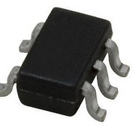
NSB1010XV5T5 ON Semiconductor, NSB1010XV5T5 Datasheet - Page 5

NSB1010XV5T5
Manufacturer Part Number
NSB1010XV5T5
Description
Digital Transistors 100mA Complementary
Manufacturer
ON Semiconductor
Datasheet
1.NSB1010XV5T5G.pdf
(6 pages)
Specifications of NSB1010XV5T5
Configuration
Dual
Transistor Polarity
NPN/PNP
Typical Input Resistor
10 KOhms at NPN, 4.7 KOhms at PNP
Typical Resistor Ratio
1
Mounting Style
SMD/SMT
Package / Case
SOT-553-5
Collector- Emitter Voltage Vceo Max
50 V
Continuous Collector Current
0.1 A
Peak Dc Collector Current
100 mA
Power Dissipation
357 mW
Maximum Operating Temperature
+ 150 C
Minimum Operating Temperature
- 55 C
Lead Free Status / RoHS Status
Lead free / RoHS Compliant
5
1
G
−X−
A
2
4
3
D
0.08 (0.003)
−Y−
5 PL
B
*For additional information on our Pb−Free strategy and soldering
details, please download the ON Semiconductor Soldering and
Mounting Techniques Reference Manual, SOLDERRM/D.
M
0.0531
X
1.35
Y
PACKAGE DIMENSIONS
SOLDERING FOOTPRINT*
5−LEAD PACKAGE
C
http://onsemi.com
CASE 463B−01
0.0197
0.0118
0.5
SOT−553
ISSUE A
0.3
0.0394
S
J
K
1.0
5
0.0197
0.5
SCALE 20:1
0.0177
0.45
inches
mm
NOTES:
1. DIMENSIONING AND TOLERANCING PER
2. CONTROLLING DIMENSION: MILLIMETERS
3. MAXIMUM LEAD THICKNESS INCLUDES
ANSI Y14.5M, 1982.
LEAD FINISH THICKNESS. MINIMUM LEAD
THICKNESS IS THE MINIMUM THICKNESS
OF BASE MATERIAL.
DIM
A
B
C
D
G
K
J
S
MILLIMETERS
MIN
1.50
1.10
0.50
0.17
0.08
0.10
1.50
0.50 BSC
MAX
1.70
1.30
0.60
0.27
0.18
0.30
1.70
0.059
0.043
0.020
0.007
0.003
0.004
0.059
MIN
0.020 BSC
INCHES
0.067
0.051
0.024
0.011
0.007
0.012
0.067
MAX


