MC33696MOD434EV Freescale Semiconductor, MC33696MOD434EV Datasheet - Page 24
MC33696MOD434EV
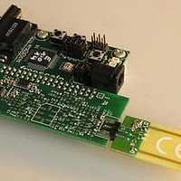
Manufacturer Part Number
MC33696MOD434EV
Description
MCU, MPU & DSP Development Tools MC33696 (ECHO) RF C EVAL
Manufacturer
Freescale Semiconductor
Specifications of MC33696MOD434EV
Processor To Be Evaluated
MC9S08RG60
Interface Type
RS-232
Lead Free Status / RoHS Status
Lead free / RoHS Compliant


Received Signal Strength Indicator (RSSI)
In OOK modulation (MODU=0), modulation is performed by switching on and off the RF output stage.
In FSK modulation (MODU = 1), modulation is performed by switching the RF carrier between two
values.
See the FRM bit description
setting carrier frequencies.
15.2 Receive Mode
The MC33696 is master and drives the digital interface in one of two ways, depending on the selection of
the data manager.
16
16.1 Module Description
In receive mode, a received signal strength indicator can be activated by setting bit RSSIE.
The input signal is measured at two different points in the receiver chain by two different means, as
follows.
24
(Output)
(Output)
SCLK
MOSI
1. DME = 1: The data manager is enabled. The SPI is master. The MC33696 sends the recovered
2. DME = 0: The data manager is disabled. The SPI is deselected. Raw data are sent directly on the
•
SEB
MOSI = 0: output stage off
MOSI = 1: output stage on
MOSI = 0: f
MOSI = 1: f
clock on SCLK and the received data on the MOSI line. Data are valid on falling edges of SCLK.
If an entire number of bytes is received, the data manager may add an extra byte. The content of
this extra byte is random. If the data received do not fill an entire number of bytes, the data manager
will fill the last byte randomly.
MOSI line, while SCLK remains at the low level.
At the IF filter output, a progressive compression logarithmic amplifier measures the input signal,
ranging from the sensitivity level up to –50 dBm.
Received Signal Strength Indicator (RSSI)
D7 D6 D5 D4
carrier0
carrier1
Recovered Clock Updated to Incoming Signal Data Rate
Figure 15. Typical Transfer in Receive Mode with Data Manager
corresponding to a logical 0
corresponding to a logical 1
D3
(Figure
D2
20) and
Figure 15
D1
MC33696 Data Sheet, Rev. 9
Section 17.3, “Frequency
D0
shows a typical transfer.
D7 D6 D5 D4 D3 D2 D1 D0 D7 D6 D5 D4 D3 D2 D1 D0
Registers,” for more details about
Freescale Semiconductor
Related parts for MC33696MOD434EV
Image
Part Number
Description
Manufacturer
Datasheet
Request
R

Part Number:
Description:
Manufacturer:
Freescale Semiconductor, Inc
Datasheet:
Part Number:
Description:
Manufacturer:
Freescale Semiconductor, Inc
Datasheet:
Part Number:
Description:
Manufacturer:
Freescale Semiconductor, Inc
Datasheet:
Part Number:
Description:
Manufacturer:
Freescale Semiconductor, Inc
Datasheet:
Part Number:
Description:
Manufacturer:
Freescale Semiconductor, Inc
Datasheet:
Part Number:
Description:
Manufacturer:
Freescale Semiconductor, Inc
Datasheet:
Part Number:
Description:
Manufacturer:
Freescale Semiconductor, Inc
Datasheet:
Part Number:
Description:
Manufacturer:
Freescale Semiconductor, Inc
Datasheet:
Part Number:
Description:
Manufacturer:
Freescale Semiconductor, Inc
Datasheet:
Part Number:
Description:
Manufacturer:
Freescale Semiconductor, Inc
Datasheet:
Part Number:
Description:
Manufacturer:
Freescale Semiconductor, Inc
Datasheet:
Part Number:
Description:
Manufacturer:
Freescale Semiconductor, Inc
Datasheet:
Part Number:
Description:
Manufacturer:
Freescale Semiconductor, Inc
Datasheet:
Part Number:
Description:
Manufacturer:
Freescale Semiconductor, Inc
Datasheet:
Part Number:
Description:
Manufacturer:
Freescale Semiconductor, Inc
Datasheet: