EA-QSB-102 Embedded Artists, EA-QSB-102 Datasheet - Page 8
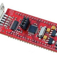
EA-QSB-102
Manufacturer Part Number
EA-QSB-102
Description
MCU, MPU & DSP Development Tools QUICKSTART PROTOTYPE BRD W/ LPC2106 RS232
Manufacturer
Embedded Artists
Specifications of EA-QSB-102
Processor To Be Evaluated
LPC2106
Data Bus Width
16 bit, 32 bit
Interface Type
RS-232, I2C, SPI, UART
Core
ARM7TDMI-S
Dimensions
27.9 mm x 65.3 mm
Maximum Operating Temperature
+ 85 C
Operating Supply Voltage
5 V
Lead Free Status / RoHS Status
Lead free / RoHS Compliant


NXP Semiconductors
Table 3.
LPC2104_2105_2106_7
Product data sheet
Symbol
P0.11/CTS1/CAP1.1
P0.12/DSR1/MAT1.0
P0.13/DTR1/MAT1.1
P0.14/DCD1/EINT1
P0.15/RI1/EINT2
P0.16/EINT0/MAT0.2
P0.17/CAP1.2/TRST
P0.18/CAP1.3/TMS
P0.19/MAT1.2/TCK
P0.20/MAT1.3/TDI
P0.21/PWM5/TDO
P0.22/TRACECLK
P0.23/PIPESTAT0
P0.24/PIPESTAT1
P0.25/PIPESTAT2
Pin description
Pin
36
37
41
44
45
46
47
48
1
2
3
32
33
34
38
[1]
[1]
[1]
[1]
[1]
[1]
[1]
[1]
[1]
[1]
[1]
[4]
[4]
[4]
[4]
…continued
Type
I/O
I
I
I/O
I
O
I/O
O
O
I/O
I
I
I/O
I
O
I/O
I
O
I/O
I
I
I/O
I
I
I/O
O
I
I/O
O
I
I/O
O
O
I/O
O
I/O
O
I/O
O
I/O
O
Description
P0.11 — Port 0 bit 11.
CTS1 — Clear to Send input for UART 1.
CAP1.1 — Capture input for Timer 1, channel 1.
P0.12 — Port 0 bit 12.
DSR1 — Data Set Ready input for UART 1.
MAT1.0 — Match output for Timer 1, channel 0.
P0.13 — Port 0 bit 13.
DTR1 — Data Terminal Ready output for UART 1.
MAT1.1 — Match output for Timer 1, channel 1.
P0.14 — Port 0 bit 14.
DCD1 — Data Carrier Detect input for UART 1.
EINT1 — External interrupt 1 input.
P0.15 — Port 0 bit 15.
RI1 — Ring Indicator input for UART 1.
EINT2 — External interrupt 2 input.
P0.16 — Port 0 bit 16.
EINT0 — External interrupt 0 input.
MAT0.2 — Match output for Timer 0, channel 2.
P0.17 — Port 0 bit 17.
CAP1.2 — Capture input for Timer 1, channel 2.
TRST — Test Reset for JTAG interface, primary JTAG pin group.
P0.18 — Port 0 bit 18.
CAP1.3 — Capture input for Timer 1, channel 3.
TMS — Test Mode Select for JTAG interface, primary JTAG pin group.
P0.19 — Port 0 bit 19.
MAT1.2 — Match output for Timer 1, channel 2.
TCK — Test Clock for JTAG interface, primary JTAG pin group.
P0.20 — Port 0 bit 20.
MAT1.3 — Match output for Timer 1, channel 3.
TDI — Test Data In for JTAG interface, primary JTAG pin group.
P0.21 — Port 0 bit 21.
PWM5 — Pulse Width Modulator output 5.
TDO — Test Data Out for JTAG interface, primary JTAG pin group.
P0.22 — Port 0 bit 22.
TRACECLK — Trace Clock. Standard I/O port with internal pull-up.
P0.23 — Port 0 bit 23.
PIPESTAT0 — Pipeline Status, bit 0. Standard I/O port with internal pull-up.
P0.24 — Port 0 bit 24.
PIPESTAT1 — Pipeline Status, bit 1. Standard I/O port with internal pull-up.
P0.25 — Port 0 bit 25.
PIPESTAT2 — Pipeline Status, bit 2. Standard I/O port with internal pull-up.
Rev. 07 — 20 June 2008
LPC2104/2105/2106
Single-chip 32-bit microcontrollers
© NXP B.V. 2008. All rights reserved.
8 of 41
Related parts for EA-QSB-102
Image
Part Number
Description
Manufacturer
Datasheet
Request
R

Part Number:
Description:
MCU, MPU & DSP Development Tools QUICKSTART PROTOTYPE BRD W/ LPC2129 CAN
Manufacturer:
Embedded Artists
Datasheet:

Part Number:
Description:
MCU, MPU & DSP Development Tools QUICKSTART PROTOTYPE BRD
Manufacturer:
Embedded Artists
Datasheet:

Part Number:
Description:
MCU, MPU & DSP Development Tools LPC2148 USB QUICKSTART BRD
Manufacturer:
Embedded Artists
Datasheet:
Part Number:
Description:
MCU, MPU & DSP Development Tools LPC2129 CAN QUICKSTART BRD
Manufacturer:
Embedded Artists
Datasheet:
Part Number:
Description:
MCU, MPU & DSP Development Tools QUICKSTART PROTOTYPE BRD W/ LPC2148
Manufacturer:
Embedded Artists
Datasheet:

Part Number:
Description:
MCU, MPU & DSP Development Tools LPC2106 RS232 QUICKSTART BRD
Manufacturer:
Embedded Artists
Datasheet:

Part Number:
Description:
BOARD QUICK START LPC1343
Manufacturer:
Embedded Artists
Datasheet:

Part Number:
Description:
Development Boards & Kits - ARM QUICK START BOARD LPC11U35
Manufacturer:
Embedded Artists
Datasheet:
Part Number:
Description:
KIT LPC3141 SODIMM 66X48 200POS
Manufacturer:
Embedded Artists
Datasheet:
Part Number:
Description:
KIT LPC3152 SODIMM 66X48 200POS
Manufacturer:
Embedded Artists
Datasheet:
Part Number:
Description:
BOARD OEM W/LPC2478 MCU
Manufacturer:
Embedded Artists
Datasheet:
Part Number:
Description:
KIT LPC3250 259 WITH QVGA
Manufacturer:
Embedded Artists
Datasheet: