EA-QSB-102 Embedded Artists, EA-QSB-102 Datasheet - Page 23
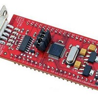
EA-QSB-102
Manufacturer Part Number
EA-QSB-102
Description
MCU, MPU & DSP Development Tools QUICKSTART PROTOTYPE BRD W/ LPC2106 RS232
Manufacturer
Embedded Artists
Specifications of EA-QSB-102
Processor To Be Evaluated
LPC2106
Data Bus Width
16 bit, 32 bit
Interface Type
RS-232, I2C, SPI, UART
Core
ARM7TDMI-S
Dimensions
27.9 mm x 65.3 mm
Maximum Operating Temperature
+ 85 C
Operating Supply Voltage
5 V
Lead Free Status / RoHS Status
Lead free / RoHS Compliant


NXP Semiconductors
LPC2104_2105_2106_7
Product data sheet
CAUTION
6.18.5 External interrupt inputs
6.18.6 Memory mapping control
6.18.7 Power control
6.18.8 APB
The LPC2104/2105/2106 include three external interrupt inputs as selectable pin
functions. The external interrupt inputs can optionally be used to wake up the processor
from Power-down mode.
The Memory mapping control alters the mapping of the interrupt vectors that appear
beginning at address 0x0000 0000. Vectors may be mapped to the bottom of the on-chip
flash memory, or to the on-chip static RAM. This allows code running in different memory
spaces to have control of the interrupts.
The LPC2104/2105/2106 support two reduced power modes: Idle mode and Power-down
mode. In Idle mode, execution of instructions is suspended until either a Reset or interrupt
occurs. Peripheral functions continue operation during Idle mode and may generate
interrupts to cause the processor to resume execution. Idle mode eliminates power used
by the processor itself, memory systems and related controllers, and internal buses.
In Power-down mode, the oscillator is shut down and the chip receives no internal clocks.
The processor state and registers, peripheral registers, and internal SRAM values are
preserved throughout Power-down mode and the logic levels of chip output pins remain
static. The Power-down mode can be terminated and normal operation resumed by either
a Reset or certain specific interrupts that are able to function without clocks. Since all
dynamic operation of the chip is suspended, Power-down mode reduces chip power
consumption to nearly zero.
The power can be controlled for each peripheral individually allowing peripherals to be
turned off if they are not needed in the application and resulting in additional power
savings.
The APB divider determines the relationship between the processor clock (CCLK) and the
clock used by peripheral devices (PCLK). The APB divider serves two purposes. The first
is to provide peripherals with the desired PCLK via APB so that they can operate at the
speed chosen for the ARM processor. In order to achieve this, the APB may be slowed
down to
power-up (and its timing cannot be altered if it does not work since the APB divider control
registers reside on the APB), the default condition at reset is for the APB to run at
3. Running an application with level CRP3 selected fully disables any access to chip via
the JTAG pins and the ISP. This mode effectively disables ISP override using P0[14]
pin, too. It is up to the user’s application to provide (if needed) a flash update
mechanism using IAP calls or a call to reinvoke ISP command to enable flash update
via UART 0.
If level three Code Read Protection (CRP3) is selected, no future factory testing can be
performed on the device.
1
2
to
1
4
of the processor clock rate. Because the APB must work properly at
Rev. 07 — 20 June 2008
LPC2104/2105/2106
Single-chip 32-bit microcontrollers
© NXP B.V. 2008. All rights reserved.
1
4
23 of 41
of the
Related parts for EA-QSB-102
Image
Part Number
Description
Manufacturer
Datasheet
Request
R

Part Number:
Description:
MCU, MPU & DSP Development Tools QUICKSTART PROTOTYPE BRD W/ LPC2129 CAN
Manufacturer:
Embedded Artists
Datasheet:

Part Number:
Description:
MCU, MPU & DSP Development Tools QUICKSTART PROTOTYPE BRD
Manufacturer:
Embedded Artists
Datasheet:

Part Number:
Description:
MCU, MPU & DSP Development Tools LPC2148 USB QUICKSTART BRD
Manufacturer:
Embedded Artists
Datasheet:
Part Number:
Description:
MCU, MPU & DSP Development Tools LPC2129 CAN QUICKSTART BRD
Manufacturer:
Embedded Artists
Datasheet:
Part Number:
Description:
MCU, MPU & DSP Development Tools QUICKSTART PROTOTYPE BRD W/ LPC2148
Manufacturer:
Embedded Artists
Datasheet:

Part Number:
Description:
MCU, MPU & DSP Development Tools LPC2106 RS232 QUICKSTART BRD
Manufacturer:
Embedded Artists
Datasheet:

Part Number:
Description:
BOARD QUICK START LPC1343
Manufacturer:
Embedded Artists
Datasheet:

Part Number:
Description:
Development Boards & Kits - ARM QUICK START BOARD LPC11U35
Manufacturer:
Embedded Artists
Datasheet:
Part Number:
Description:
KIT LPC3141 SODIMM 66X48 200POS
Manufacturer:
Embedded Artists
Datasheet:
Part Number:
Description:
KIT LPC3152 SODIMM 66X48 200POS
Manufacturer:
Embedded Artists
Datasheet:
Part Number:
Description:
BOARD OEM W/LPC2478 MCU
Manufacturer:
Embedded Artists
Datasheet:
Part Number:
Description:
KIT LPC3250 259 WITH QVGA
Manufacturer:
Embedded Artists
Datasheet: