KIT34844AEPEVBE Freescale Semiconductor, KIT34844AEPEVBE Datasheet - Page 48
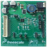
KIT34844AEPEVBE
Manufacturer Part Number
KIT34844AEPEVBE
Description
LED Lighting Development Kits IC, 10 CHANNEL LED BACKLIGHT
Manufacturer
Freescale Semiconductor
Datasheet
1.MC34844AEP.pdf
(62 pages)
Specifications of KIT34844AEPEVBE
Supply Voltage
12 V
Supply Current
2 uA
For Use With/related Products
34844A
Lead Free Status / RoHS Status
Lead free / RoHS Compliant


NORMAL MODE
drive up to 50 mA of current through each one of the LED
channels. The 34844A can be configured in master or slave
mode as set by the M/~S pin.
programmed through the I
value sets the number of 27 kHz clocks (37μs) in one PWM
cycle. The 18-bit resolution allows minimum PWM
frequencies of 110 Hz to be programmed. The resulting
frequency is output on the CK pin.
digital PLL uses this frequency as the PWM frequency.
output to the input on a number of slave configured devices,
all PWM frequencies are synchronized together. For this
application A0/SEN pin indicates which device is enable for
I
internal PWM generator period to the period of the signal
present at the CK pin. The PLL can lock to any frequency
from 110 Hz to 27 KHz provided the jitter is below 1000 ppm.
At frequencies above 1.0 KHz, the PLL will maintain lock
regardless of the transient power conditions imposed by the
user (i.e. going from 0% duty cycle to 100% at 20W LED
display power). Below 1.0 kHz, thermal time constants on the
die are such that the PLL may momentarily lose lock if the die
temperature changes substantially during a large load power
step. As explained below, this anomaly can be avoided by
controlling the rate of change in PWM duty cycle.
PLL uses a VCO that is subject to thermal drift on the order
of 1000 ppm/C. Further consider that the thermal time
constant of the chip is on the order of single digit
milliseconds. Therefore, if a large power load step is imposed
by the user (i.e. going from 0% duty cycle to 100% duty cycle
with a load power of 20 W), the die will experience a large
temperature wave gradient that will propagate across the
chip surface and thereby affect the instantaneous frequency
of the VCO. As long as such changes are within the
bandwidth of the PLL, the PLL will be able to track and
maintain lock. Exceeding this rate of change may cause the
PLL to lose lock and the backlight will momentarily be
blanked until lock is reacquired.
10 Hz. This means that temperature changes on the order of
100 ms are tolerable without losing lock. But full load power
changes on the order of 10 ms (i.e. 110 Hz PWM) are not
tracked out and the PLL can momentarily lose lock. If this
happens, as stated above, the LED drivers are momentarily
disabled until lock is reacquired. This will be manifested as a
perceivable short flash on the backlight immediately after the
load change.
48
34844A
FUNCTIONAL DEVICE OPERATION
OPERATIONAL MODES
2
C control.
In normal operation the 34844A is programed via I
In Master mode, the internal PWM generator frequency is
In slave mode, the CK pin acts as an input. The internal
By setting one device as a master, and connecting the CK
In Slave mode, an internal phase lock loop will lock the
To better understand this issue, consider that the on chip
At 110 Hz lock, the PLL has a bandwidth of approximately
2
C interface. The programmed
FUNCTIONAL DEVICE OPERATION
OPERATIONAL MODES
2
C to
instantaneous changes in die temperature by invoking only
small power steps when raising or lowering the display power
at low PWM frequencies. For example, to maintain lock while
transitioning from 0% to 100% duty cycle at 20 W load power
and a PWM frequency of 110 Hz would entail stepping the
power at a rate not to exceed 1% per 10 ms. If a load of less
than 20 W is used, then the rate of rise can be increased. As
the locked PWM frequency increases (i.e. use 600 Hz
instead of 110 Hz), the step rate can be further increased to
approximately 4% per 2.0 ms. The exact step rate to avoid
loss of PLL lock is a function of essentially three things: (a)
the composite thermal resistance of the user's PCB
assembly, (b) the load power, and (c) the PWM frequency.
For all cases below 1.0 KHz, simply using a rate of 1% duty
cycle change per PWM period will be adequate. If this is too
slow, the value can be optimized experimentally once the
hardware design is complete. At PWM rates above 1.0 KHz,
it is not necessary to control the rate of change in PWM duty
cycle.
master mode, one does not need to concern themselves with
loss of lock since the reference clock and the VCO clock are
collocated on the die, and therefore experience the same
thermal shift. Hence in master mode, once lock is initially
acquired, it is not lost and no blanking of the display occurs.
is set using a second register on the I
pin. This pin is AND’ed with the internal signal, giving the
ability to control the duty cycle either via I
setting any of the 2 signals to 100% duty cycle.
MANUAL MODE
using the I
dimming will be controlled by the external PWM signal. The
over-voltage protection limit can be settled by a resistor
divider or a zener diode on A0/SEN pin.
Configuration, refer
PIN and NIN pins are enabled to scale the current capability
per string and may be disable by setting 2.2 V in the
corresponding terminal.
will be in charge of controlling the LED dimming and a second
signal will enable or disable the chip through the EN pin.
SDA pin. The PWM signal applied to PWM pin will be in
To avoid this problem, one can simply limit large
It is important to point out that when operating in the
The duty cycle of the PWM in both master and slave mode
An external PWM signal can also be applied in the PWM
The 34844A can also be used in Manual mode without
During manual mode, all internal Registers are in Default
Also in this mode, the device can be enabled as follows:
• EN pin + PWM signal (Two Signals):
In this configuration, the PWM signal applied to PWM pin
• PWM Signal tied to SDA pin (Just ONE signal):
In this configuration the PWM pin should be tied to the
2
C interface. By setting the pin M/~S High, the LED
Table
Analog Integrated Circuit Device Data
14, under this configuration the
Freescale Semiconductor
2
C interface.
2
C or externally by
Related parts for KIT34844AEPEVBE
Image
Part Number
Description
Manufacturer
Datasheet
Request
R

Part Number:
Description:
Manufacturer:
Freescale Semiconductor, Inc
Datasheet:
Part Number:
Description:
Manufacturer:
Freescale Semiconductor, Inc
Datasheet:
Part Number:
Description:
Manufacturer:
Freescale Semiconductor, Inc
Datasheet:
Part Number:
Description:
Manufacturer:
Freescale Semiconductor, Inc
Datasheet:
Part Number:
Description:
Manufacturer:
Freescale Semiconductor, Inc
Datasheet:
Part Number:
Description:
Manufacturer:
Freescale Semiconductor, Inc
Datasheet:
Part Number:
Description:
Manufacturer:
Freescale Semiconductor, Inc
Datasheet:
Part Number:
Description:
Manufacturer:
Freescale Semiconductor, Inc
Datasheet:
Part Number:
Description:
Manufacturer:
Freescale Semiconductor, Inc
Datasheet:
Part Number:
Description:
Manufacturer:
Freescale Semiconductor, Inc
Datasheet:
Part Number:
Description:
Manufacturer:
Freescale Semiconductor, Inc
Datasheet:
Part Number:
Description:
Manufacturer:
Freescale Semiconductor, Inc
Datasheet:
Part Number:
Description:
Manufacturer:
Freescale Semiconductor, Inc
Datasheet:
Part Number:
Description:
Manufacturer:
Freescale Semiconductor, Inc
Datasheet:
Part Number:
Description:
Manufacturer:
Freescale Semiconductor, Inc
Datasheet: