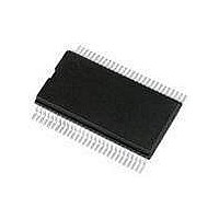
PCF8579TD NXP Semiconductors, PCF8579TD Datasheet - Page 7

PCF8579TD
Manufacturer Part Number
PCF8579TD
Description
LCD Drivers LCD DRVR DOT MATRIX
Manufacturer
NXP Semiconductors
Datasheet
1.PCF8579T1112.pdf
(41 pages)
Specifications of PCF8579TD
Maximum Clock Frequency
10 KHz
Operating Supply Voltage
2.5 V to 6 V
Maximum Power Dissipation
400 mW
Package / Case
VSO-56
Maximum Supply Current
20 uA
Lead Free Status / RoHS Status
Lead free / RoHS Compliant
Other names
PCF8579T/1,112
NXP Semiconductors
8. Functional description
PCF8579_5
Product data sheet
7.2 Pin description
8.1 Power-on reset
Table 3.
[1]
[2]
The PCF8579 column driver is designed for use with the PCF8578. Together they form a
general purpose LCD dot matrix chip set.
Typically up to 16 PCF8579s may be used with one PCF8578 (examples of cascading the
devices see
PCF8579s is identified by a unique 4-bit hardware subaddress, set by pins A0 to A3.
The PCF8578 can operate with up to 32 PCF8579s when using two I
addresses. The two slave addresses are set by the logic level on input SA0.
At power-on the PCF8579 resets to a defined starting condition as follows:
Symbol
SDA
SCL
SYNC
CLK
V
TEST
SA0
A3 to A0
V
n.c.
V
V
C39 to C0
1. Display blank (in conjunction with PCF8578)
2. 1:32 multiplex rate
3. Start bank 0 selected
4. Data pointer is set to X, Y address 0, 0
5. Character mode
6. Subaddress counter is set to 0
7. I
SS
DD
3
LCD
, V
[2]
The TEST pin must be connected to V
Do not connect, these pins are reserved.
2
4
[1]
C-bus interface is initialized
Pin description
Table
16,
Pin
VSO56
1
2
3
4
5
6
7
8 to 11
12
13
14, 15
16
17 to 56
Figure
Rev. 05 — 11 May 2009
21,
Figure
SS
LCD column driver for dot matrix graphic displays
LQFP64,
TQFP64
7
8
9
10
11
12
13
14, 16 to 18
20
15, 19, 21, 25
to 29, 34
22, 23
24
30 to 33, 35
to 64, 1 to 6
.
22,
Figure 23
Description
I
I
cascade synchronization output
external clock input/output
ground
test pin
I
I
supply voltage
not connected
LCD bias voltage inputs
LCD supply voltage
LCD column driver outputs
2
2
2
2
C-bus serial data input/output
C-bus serial clock input
C-bus slave address input (bit 0)
C-bus subaddress inputs
and
Figure
24). Each of the
2
C-bus slave
PCF8579
© NXP B.V. 2009. All rights reserved.
7 of 41


