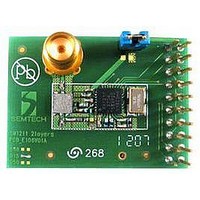
SM1211E915 Semtech, SM1211E915 Datasheet - Page 73

SM1211E915
Manufacturer Part Number
SM1211E915
Description
Dev Kit Accessory
Manufacturer
Semtech
Specifications of SM1211E915
Modulation Type
FSK, OOK
Data Rate Max
200Kbps
Frequency Range
902MHz To 928MHz
Supply Voltage Range
2.1V To 3.6V
Module Interface
SPI
Supply Current
25mA
Accessory Type
RF Module
Sensitivity
-105dBm
Operating Temperature (min)
-40C
Operating Temperature (max)
85C
Operating Temperature Classification
Industrial
Package Type
TQFN EP
Operating Supply Voltage (min)
2.1V
Operating Supply Voltage (typ)
2.5/3.3V
Operating Supply Voltage (max)
3.6V
Sensitivity (dbm)
-105dBm
Rohs Compliant
NA
Lead Free Status / RoHS Status
na
Lead Free Status / RoHS Status
na
It is recommended that this reference design (i.e. schematics, placement, layout, BOM,) is replicated in the final
application board to guarantee optimum performance.
The reference design area is represented by the dashed rectangle. C12 is a DC blocking capacitor which protects
the SAW filter. It has been added for debug purposes could be removed for a direct antenna connection if there is
no DC bias is expected at the antenna port. Please note that C10 and C11 are not used.
As illustrated in figures below, the layout has the following characteristics:
Rev 7 – Sept 2
ADVANCED COMMUNICATIONS & SENSING
7.5. Reference Design
very compact (9x19mm) => can be easily inserted even on very small PCBs
standard PCB technology (2 layers, 1.6mm, std via & clearance) => low cost
Its performance is quasi-insensitive to dielectric thickness => minimal design effort to transfer to other PCB
technologies (thickness, # of layers, etc...)
7.5.1. Application Schematic
7.5.2. PCB Layout
nd
, 2008
Figure 56: Reference Design Circuit Schematic
Page 73 of 92
www.semtech.com
SX1211


