DK-START-4CGX15N/P Altera, DK-START-4CGX15N/P Datasheet - Page 28
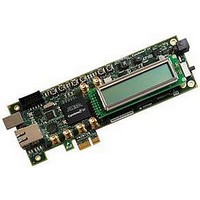
DK-START-4CGX15N/P
Manufacturer Part Number
DK-START-4CGX15N/P
Description
Cyclone IV Tranceiver Development Kit
Manufacturer
Altera
Datasheet
1.DK-START-4CGX15N.pdf
(40 pages)
Specifications of DK-START-4CGX15N/P
Silicon Manufacturer
Altera
Features
System Controller Enabling Passive Serial, Flash/SRAM Memory Devices, PCI Express Edge Connector
Kit Contents
Board, Cables, PSU, CD
Core Architecture
FPGA
Core Sub-architecture
Cyclone
Silicon Core Number
EP4C
Silicon Family Name
Cyclone IV GX
Rohs Compliant
Yes
Lead Free Status / RoHS Status
Lead free / RoHS Compliant


2–20
Table 2–24. PCI Express Pin Assignments, Schematic Signal Names, and Functions
Cyclone IV GX Transceiver Starter Board Reference Manual
Board Reference
U14.A16
U14.A17
U14.B14
U14.B15
U14.A13
U14.A14
U14.A11
U14.B17
U14.A1
U14.A5
U14.A6
U14.A7
U14.A8
Add-in card transmit bus
Add-in card transmit bus
Add-in card receive bus
Add-in card receive bus
Motherboard reference clock
Motherboard reference clock
Reset
Present
x1 Present
Motherboard TCK
Motherboard TDI
Motherboard TDO
Motherboard TMS
The PCI Express interface supports a channel width of ×1 as well as the connection
speed of Gen1 at 2.5 Gbps/lane.
The board’s power can be sourced entirely from the PCI Express edge connector when
installed into a PC motherboard. Turn the power switch (SW1) to ON position when
you install the board into a PC motherboard. Although the board can also be powered
by a laptop power supply for use on a lab bench, it is not recommended to use from
both supplies at the same time. Ideal diode power sharing devices have been
designed into this board to prevent damages or back-current from one supply to the
other.
The PCIE_REFCLK_P and PCIE_REFCLK_N signals are a 100-MHz differential input
that is driven from the PC motherboard on this board through the PCI Express edge
connector. This signal connects directly to a Cyclone IV GX REFCLK input pin pair.
This clock is terminated on the motherboard and therefore, no on-board termination is
required. This clock can have spread-spectrum properties that change its period
between 9.847 ps to 10.203 ps. The I/O standard is High-Speed Current Steering Logic
(HCSL).
By default, the GXB_RX0 channel of the FPGA is connected to the PCIE_RX_P and
PCIE_RX_N signals, while the GXB_TX0 channel is connected to the PCIE_TX_P and
PCIE_TX_N signals.
Table 2–24
directions are relative to the Cyclone IV GX FPGA.
Description
summarizes the PCI Express pin assignments. The signal names and
PCIE_TX_P
PCIE_TX_N
PCIE_RX_P
PCIE_RX_N
PCIE_REFCLK_P
PCIE_REFCLK_N
PCIE_PERSTn
PCIE_PRSNTn_x1
PCIE_PRSNTn_x1
PCIE_JTAG_TCK
PCIE_JTAG_TDI
PCIE_JTAG_TDO
PCIE_JTAG_TMS
Schematic Signal Name
I/O Standard
1.4-V PCML
LVTTL
Components and Transceiver Interfaces
HCSL
3.3-V
—
—
© March 2010 Altera Corporation
Chapter 2: Board Components
Cyclone IV GX
Pin Number
Device
A10
G2
G1
J2
J1
J6
J7
—
—
—
—
—
—
Related parts for DK-START-4CGX15N/P
Image
Part Number
Description
Manufacturer
Datasheet
Request
R

Part Number:
Description:
KIT STARTER CYCLONE III EP3C25
Manufacturer:
Altera
Datasheet:

Part Number:
Description:
KIT STARTER CYCLONE IV GX
Manufacturer:
Altera
Datasheet:

Part Number:
Description:
Programmable Logic IC Development Tools FPGA Development Kit For 5AGXFB3H4F35C5N
Manufacturer:
Altera Corporation
Datasheet:
Part Number:
Description:
Programmable Logic IC Development Tools FPGA Starter Kit For 5AGXFB3H4F
Manufacturer:
Altera Corporation
Datasheet:

Part Number:
Description:
KIT, DEV, PCI EXPRESS, ECP2M
Manufacturer:
LATTICE SEMICONDUCTOR

Part Number:
Description:
CYCLONE II STARTER KIT EP2C20N
Manufacturer:
Altera
Datasheet:

Part Number:
Description:
CPLD, EP610 Family, ECMOS Process, 300 Gates, 16 Macro Cells, 16 Reg., 16 User I/Os, 5V Supply, 35 Speed Grade, 24DIP
Manufacturer:
Altera Corporation
Datasheet:
Part Number:
Description:
CPLD, EP610 Family, ECMOS Process, 300 Gates, 16 Macro Cells, 16 Reg., 16 User I/Os, 5V Supply, 15 Speed Grade, 24DIP
Manufacturer:
Altera Corporation
Datasheet:
Part Number:
Description:
Manufacturer:
Altera Corporation
Datasheet:
Part Number:
Description:
CPLD, EP610 Family, ECMOS Process, 300 Gates, 16 Macro Cells, 16 Reg., 16 User I/Os, 5V Supply, 30 Speed Grade, 24DIP
Manufacturer:
Altera Corporation
Datasheet:
Part Number:
Description:
High-performance, low-power erasable programmable logic devices with 8 macrocells, 10ns
Manufacturer:
Altera Corporation
Datasheet:
Part Number:
Description:
High-performance, low-power erasable programmable logic devices with 8 macrocells, 7ns
Manufacturer:
Altera Corporation
Datasheet:
Part Number:
Description:
Classic EPLD
Manufacturer:
Altera Corporation
Datasheet: