DK-START-4CGX15N/P Altera, DK-START-4CGX15N/P Datasheet - Page 13
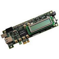
DK-START-4CGX15N/P
Manufacturer Part Number
DK-START-4CGX15N/P
Description
Cyclone IV Tranceiver Development Kit
Manufacturer
Altera
Datasheet
1.DK-START-4CGX15N.pdf
(40 pages)
Specifications of DK-START-4CGX15N/P
Silicon Manufacturer
Altera
Features
System Controller Enabling Passive Serial, Flash/SRAM Memory Devices, PCI Express Edge Connector
Kit Contents
Board, Cables, PSU, CD
Core Architecture
FPGA
Core Sub-architecture
Cyclone
Silicon Core Number
EP4C
Silicon Family Name
Cyclone IV GX
Rohs Compliant
Yes
Lead Free Status / RoHS Status
Lead free / RoHS Compliant


Chapter 2: Board Components
Featured Device: Cyclone IV GX Device
I/O Resources
Figure 2–2. EP4CGX15BF14 Device I/O Bank Diagram
Table 2–4. Cyclone IV GX Device I/O Pin Count and Usage
© March 2010 Altera Corporation
Flash, SSRAM, FSML Bus
Gigabit Ethernet
Buttons
LCD
LEDs
Clocks or Oscillators
PCI Express
Passive serial and active serial
configuration
Device I/O Total:
Notes to
(1) 60 out of 72 user I/Os are bidirectional I/O pins while the other 12 pins are for clock inputs only.
(2) The total I/O count excludes the transceiver bank.
Table
Function
2–4:
Figure 2–2
device in the 169-pin FBGA package.
Table 2–4
starter board.
of Channels
Number
2
Name
Bank
GXB0
lists the Cyclone IV GX device pin count and usage by function on the
illustrates the bank organization and I/O count for the EP4CGX15BF14
2.5-V CMOS + LVDS
I/O Standard
2.5-V CMOS
2.5-V CMOS
EP4CGX15
(Note 1)
I/O Count
71/72
47
4
3
1
4
7
1
4
(2)
Cyclone IV GX Transceiver Starter Board Reference Manual
Bank 6A
Bank 5A
1 DEV_OE
—
1 DEV_CLRn
—
1 INIT_DONE, 1 nCEO
3 differential clock input pair, 1 clock input
—
—
Name
Bank
Number
of I/Os
12
12
Special Pins
2–5
Related parts for DK-START-4CGX15N/P
Image
Part Number
Description
Manufacturer
Datasheet
Request
R

Part Number:
Description:
KIT STARTER CYCLONE III EP3C25
Manufacturer:
Altera
Datasheet:

Part Number:
Description:
KIT STARTER CYCLONE IV GX
Manufacturer:
Altera
Datasheet:

Part Number:
Description:
Programmable Logic IC Development Tools FPGA Development Kit For 5AGXFB3H4F35C5N
Manufacturer:
Altera Corporation
Datasheet:
Part Number:
Description:
Programmable Logic IC Development Tools FPGA Starter Kit For 5AGXFB3H4F
Manufacturer:
Altera Corporation
Datasheet:

Part Number:
Description:
KIT, DEV, PCI EXPRESS, ECP2M
Manufacturer:
LATTICE SEMICONDUCTOR

Part Number:
Description:
CYCLONE II STARTER KIT EP2C20N
Manufacturer:
Altera
Datasheet:

Part Number:
Description:
CPLD, EP610 Family, ECMOS Process, 300 Gates, 16 Macro Cells, 16 Reg., 16 User I/Os, 5V Supply, 35 Speed Grade, 24DIP
Manufacturer:
Altera Corporation
Datasheet:
Part Number:
Description:
CPLD, EP610 Family, ECMOS Process, 300 Gates, 16 Macro Cells, 16 Reg., 16 User I/Os, 5V Supply, 15 Speed Grade, 24DIP
Manufacturer:
Altera Corporation
Datasheet:
Part Number:
Description:
Manufacturer:
Altera Corporation
Datasheet:
Part Number:
Description:
CPLD, EP610 Family, ECMOS Process, 300 Gates, 16 Macro Cells, 16 Reg., 16 User I/Os, 5V Supply, 30 Speed Grade, 24DIP
Manufacturer:
Altera Corporation
Datasheet:
Part Number:
Description:
High-performance, low-power erasable programmable logic devices with 8 macrocells, 10ns
Manufacturer:
Altera Corporation
Datasheet:
Part Number:
Description:
High-performance, low-power erasable programmable logic devices with 8 macrocells, 7ns
Manufacturer:
Altera Corporation
Datasheet:
Part Number:
Description:
Classic EPLD
Manufacturer:
Altera Corporation
Datasheet: