78Q2123-DB TERIDIAN, 78Q2123-DB Datasheet - Page 5
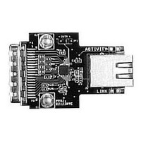
78Q2123-DB
Manufacturer Part Number
78Q2123-DB
Description
Development Tools & Eval/Demo Boards
Manufacturer
TERIDIAN
Datasheet
1.78Q2133-DB.pdf
(13 pages)
Specifications of 78Q2123-DB
Silicon Manufacturer
Teridian
Application Sub Type
MII
Kit Application Type
Interface
Silicon Core Number
78Q2123
Lead Free Status / RoHS Status
Lead free / RoHS Compliant


PCB Layout Considerations
The following recommendations enhance the MicroPHY’s performance while minimizing EMC emissions:
1.
2.
3.
4.
5.
6.
7.
8.
9.
10.
11.
12.
13.
14.
15.
16.
17.
18.
19.
20.
21.
22.
23.
24.
© 2006 Teridian Semiconductor Corporation, Proprietary and Confidential
The transformer to transceiver signal traces must be 100Ω differential transmission lines.
Place the termination network components near the input data pins of the transceiver or transformer.
Make all differential signal pairs short and of the same length.
Decouple the transceiver thoroughly with 0.01µF and 0.1µF capacitors.
Locate these decoupling capacitors as close as possible to the respective transceiver VCC and GND
pins.
All decoupling capacitor and transceiver VCC and GND connections should tie immediately to a VCC or
GND plane via with minimum trace inductance.
Total decoupling capacitance should be greater than the load capacitance that the digital output drivers
must drive.
Use low inductance, ceramic surface mount decoupling capacitors.
Use a multi-layer PCB with the inner layers dedicated to GND and VCC.
A single VCC and GND plane is recommended for optimum performance. The lowest possible series
impedance is required between the analog and digital VCC and GND pins respectively of the transceiver.
The outer layers of a 4 layer PCB are to be used for signal routing.
Place the highest speed signals on the layer adjacent to the GND plane.
Physically separate the analog signals from the digital signals by placing them on opposite layers or
routing them away from each other.
Additional component and solder side ground layers may be added for maximum EMC containment.
The GND plane should extend out to the transceiver side of the transformer. Remove the VCC and GND
planes from the line side of the transformer to the RJ-45 connector.
Do not allow the chassis ground plane to cross over the transceiver GND plane. Minimum separation
must accommodate over 1.5kV.
Provide onboard termination of the unused signal pairs in the CAT-5 cable.
Use a shielded RJ-45 connector with its case stakes soldered to the chassis ground.
Locate the transformer adjacent to the RJ-45 to minimize the shunt capacitance to the line.
Minimize RF current fringing by making the VCC plane 0.10 inch smaller than the GND plane. If multiple
transceivers are used, provide partitions in the VCC and GND planes between the analog sections.
Maintain the partition from the transformer up to the transceiver’s analog interface. Do not cross these
partitions with signal traces, in particular any digital signals from adjacent transceivers.
Add series resistors on all transceiver MII outputs to minimize digital output driver peak currents.
Minimize the use of vias when routing the analog signal traces.
Isolate the crystal and its capacitors from the analog signals with a guard ring.
The crystal compensation capacitor value (C2 & C3) must be selected to trim the oscillator’s frequency to
25.0000 MHz ±50ppm. The optimum value will be layout dependent. A mere ±4pF can shift the 25MHz
±100Hz. The 25.0000 MHz ±50ppm is specified by the IEEE.
Note: System vendors need to select the proper crystal according to their applications, such as operating
environment, product lifetime, and etc since crystal aging, operating temperature, and other factors can
affect the crystal frequency tolerance.
- 5 -
DEMO BOARD MANUAL
78Q21x3-DB MicroPHY
MII Evaluation Board
Rev_2.2
TM
fd
Related parts for 78Q2123-DB
Image
Part Number
Description
Manufacturer
Datasheet
Request
R

Part Number:
Description:
10/100BASE-TX Transceiver
Manufacturer:
TERIDIAN [Teridian Semiconductor Corporation]
Datasheet:
Part Number:
Description:
Low Power Ethernet Coaxial Transceiver
Manufacturer:
TERIDIAN [Teridian Semiconductor Corporation]
Datasheet:
Part Number:
Description:
2-port E3/DS3/STS-1 LIU with Jitter Attenuator
Manufacturer:
TERIDIAN [Teridian Semiconductor Corporation]
Datasheet:
Part Number:
Description:
3-port E3/DS3/STS-1 LIU with Jitter Attenuator
Manufacturer:
TERIDIAN [Teridian Semiconductor Corporation]
Datasheet:
Part Number:
Description:
4-port E3/DS3/STS-1 LIU with Jitter Attenuator
Manufacturer:
TERIDIAN [Teridian Semiconductor Corporation]
Datasheet:
Part Number:
Description:
Single Channel OC-3/ STM1-E/ E4 LIU
Manufacturer:
TERIDIAN [Teridian Semiconductor Corporation]
Datasheet:
Part Number:
Description:
Serial 155M NRZ to CMI Converter
Manufacturer:
TERIDIAN [Teridian Semiconductor Corporation]
Datasheet:
Part Number:
Description:
Dual Channel OC-3/ STM1-E/ E4 LIU
Manufacturer:
TERIDIAN [Teridian Semiconductor Corporation]
Datasheet:
Part Number:
Description:
Electronic Trip Unit
Manufacturer:
TERIDIAN [Teridian Semiconductor Corporation]
Datasheet:
Part Number:
Description:
Single-Phase Energy Meter IC
Manufacturer:
TERIDIAN [Teridian Semiconductor Corporation]
Datasheet:
Part Number:
Description:
Energy Meter IC
Manufacturer:
TERIDIAN [Teridian Semiconductor Corporation]
Datasheet:
Part Number:
Description:
Energy Meter IC
Manufacturer:
TERIDIAN [Teridian Semiconductor Corporation]
Datasheet:
Part Number:
Description:
Split-Phase Evaluation Board Power, current, voltage and power factor indicator dials
Manufacturer:
TERIDIAN [Teridian Semiconductor Corporation]
Part Number:
Description:
Single-Phase AC Power Measurement IC
Manufacturer:
TERIDIAN [Teridian Semiconductor Corporation]
Datasheet:
Part Number:
Description:
IC, ETHERNET TXRX, IEEE 802.3, LQFP-100
Manufacturer:
TERIDIAN
Datasheet: