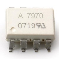
ACPL-7970-500E Avago Technologies US Inc., ACPL-7970-500E Datasheet - Page 15

ACPL-7970-500E
Manufacturer Part Number
ACPL-7970-500E
Description
IsolatedSigmaDelta Mod, TR+IEC+LF
Manufacturer
Avago Technologies US Inc.
Series
-r
Type
Sigma-Delta Modulatorr
Datasheet
1.ACPL-7970-000E.pdf
(18 pages)
Specifications of ACPL-7970-500E
Operating Supply Voltage
5.5 V
Supply Current
8 mA at 5 V
Operating Temperature Range
- 40 C to + 105 C
Mounting Style
SMD/SMT
Package / Case
DIP-8 Gull Wing
Input Voltage Range (max)
+ 200 mV
Voltage - Isolation
5000Vrms
Input Type
DC
Voltage - Supply
3 V ~ 5.5 V, 4.5 V ~ 5.5 V
Operating Temperature
-40°C ~ 105°C
Mounting Type
Surface Mount
Lead Free Status / Rohs Status
Details
Available stocks
Company
Part Number
Manufacturer
Quantity
Price
Power Supplies and Bypassing
As shown in Figure 19, a floating power supply (which in
many applications could be the same supply that is used
to drive the high-side power transistor) is regulated to
5 V using a simple zener diode (D1); the value of resistor
R1 should be chosen to ensure sufficient current can be
supplied from the existing floating supply. The voltage
from the current sensing resistor or shunt (R
applied to the input of the ACPL-7970 through an RC anti-
aliasing filter (R2 and C2). And finally, a clock is connected
to the ACPL-7970 and data are connected to the digital
filter. Although the application circuit is relatively simple,
a few recommendations should be followed to ensure
optimal performance.
The power supply for the isolated modulator is most often
obtained from the same supply used to power the power
transistor gate drive circuit. If a dedicated supply is required,
in many cases it is possible to add an additional winding
on an existing transformer. Otherwise, some sort of simple
isolated supply can be used, such as a line powered trans-
former or a high-frequency DC-DC converter.
An inexpensive 78L05 three terminal regulator can also be
used to reduce the floating supply voltage to 5 V. To help
attenuate high-frequency power supply noise or ripple, a
resistor or inductor can be used in series with the input of
the regulator to form a low-pass filter with the regulator’s
input bypass capacitor.
As shown in Figure 19, bypass capacitors (C1a, C1b, C3a
and C3b) should be located as close as possible to the
input and output power-supply pins of the isolated
modulator. The bypass capacitors are required because
of the high-speed digital nature of the signals inside the
isolated modulator. A bypass capacitor (C2) is also recom-
mended at the input due to the switched-capacitor nature
of the input circuit. The input bypass capacitor also forms
part of the anti-aliasing filter, which is recommended to
prevent high frequency noise from aliasing down to lower
frequencies and interfering with the input signal.
Figure 20. Motor Output Horsepower vs. Motor Phase Current and Supply.
15
40
35
30
25
20
15
10
5
0
0
5
440 V
380 V
220 V
120 V
MOTOR PHASE CURRENT - A (rms)
10
15
20
25
30
SENSE
35
) is
PC Board Layout
The design of the printed circuit board (PCB) should follow
good layout practices, such as keeping bypass capacitors
close to the supply pins, keeping output signals away from
input signals, the use of ground and power planes, etc. In
addition, the layout of the PCB can also affect the isolation
transient immunity (CMR) of the isolated modulator, due
primarily to stray capacitive coupling between the input
and the output circuits. To obtain optimal CMR perfor-
mance, the layout of the PC board should minimize any
stray coupling by maintaining the maximum possible
distance between the input and output sides of the circuit
and ensuring that any ground or power plane on the PC
board does not pass directly below or extend much wider
than the body of the isolated modulator.
Shunt Resistors
The current-sensing shunt resistor should have low re-
sistance (to minimize power dissipation), low inductance
(to minimize di/dt induced voltage spikes which could
adversely affect operation), and reasonable tolerance (to
maintain overall circuit accuracy). Choosing a particu-
lar value for the shunt is usually a compromise between
minimizing power dissipation and maximizing accuracy.
Smaller shunt resistances decrease power dissipation,
while larger shunt resistances can improve circuit accuracy
by utilizing the full input range of the isolated modulator.
The first step in selecting a shunt is determining how
much current the shunt will be sensing. The graph in
Figure 20 shows the RMS current in each phase of a three-
phase induction motor as a function of average motor
output power (in horsepower, hp) and motor drive supply
voltage. The maximum value of the shunt is determined
by the current being measured and the maximum recom-
mended input voltage of the isolated modulator. The
maximum shunt resistance can be calculated by taking
the maximum recommended input voltage and dividing
by the peak current that the shunt should see during
normal operation. For example, if a motor will have a
maximum RMS current of 10 A and can experience up to
50% overloads during normal operation, then the peak
current is 21.1 A (= 10 x 1.414 x 1.5). Assuming a maximum
input voltage of 200 mV, the maximum value of shunt
resistance in this case would be about 10 m:.
The maximum average power dissipation in the shunt
can also be easily calculated by multiplying the shunt re-
sistance times the square of the maximum RMS current,
which is about 1 W in the previous example.


