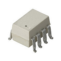
HCPL-2602-300E Avago Technologies US Inc., HCPL-2602-300E Datasheet - Page 9

HCPL-2602-300E
Manufacturer Part Number
HCPL-2602-300E
Description
OPTOCOUPLER, TRANSISTOR, 3750VRMS
Manufacturer
Avago Technologies US Inc.
Type
Line Receiverr
Datasheet
1.HCPL-2612-000E.pdf
(16 pages)
Specifications of HCPL-2602-300E
No. Of Channels
1
Optocoupler Output Type
Logic Gate
Input Current
60mA
Output Voltage
5.5V
Opto Case Style
SMD
No. Of Pins
8
Peak Reflow Compatible (260 C)
Yes
Isolation Voltage
3.75kV
Voltage - Isolation
3750Vrms
Input Type
AC, DC
Voltage - Supply
4.5 V ~ 5.5 V
Operating Temperature
0°C ~ 70°C
Mounting Type
Surface Mount
Package / Case
8-SMD Gull Wing
Number Of Elements
1
Output Type
Open Collector
Baud Rate
10Mbps
Forward Voltage
2.7V
Forward Current
60mA
Output Current
50mA
Package Type
PDIP SMD
Operating Temp Range
0C to 70C
Power Dissipation
40mW
Propagation Delay Time
75ns
Pin Count
8
Mounting
Surface Mount
Reverse Breakdown Voltage
0.95V
Operating Temperature Classification
Commercial
Lead Free Status / RoHS Status
Lead free / RoHS Compliant
Lead Free Status / RoHS Status
Lead free / RoHS Compliant, Lead free / RoHS Compliant
Available stocks
Company
Part Number
Manufacturer
Quantity
Price
Company:
Part Number:
HCPL-2602-300E
Manufacturer:
AVAGO
Quantity:
30 000
Notes:
10. No external pull up is required for a high logic state on the enable input. If the V
11. In accordance with UL 1577, each optocoupler is proof tested by applying an insulation test voltage of 4500 for one second (leakage detection
12. t
13. See application section titled “Propagation Delay, Pulse-Width Distortion and Propagation Delay Skew” for more information.
Figure 1. Typical high level output current vs.
temperature.
Figure 4. Typical output voltage vs. forward
input current.
9
1. Bypassing of the power supply line is required, with a 0.1 F ceramic disc capacitor adjacent to each optocoupler as illustrated in Figure 15. Total
2. Device considered a two terminal device: pins 1, 2, 3, and 4 shorted together, and pins 5, 6, 7, and 8 shorted together.
3. The t
4. The t
5. The t
6. The t
7. CM
8. CM
9. For sinusoidal voltages,
15
10
lead length between both ends of the capacitor and the isolator pins should not exceed 20 mm.
output pulse.
output pulse.
of the output pulse.
of the output pulse.
performance.
current limit, I
range.
6
3
2
1
0
5
0
5
4
PSK
-60
0
I
F
H
L
is equal to the worst case difference in t
– FORWARD INPUT CURRENT – mA
is the maximum tolerable rate of fall of the common mode voltage to assure that the output will remain in a low logic state (i.e., V
PLH
PHL
ELH
EHL
is the maximum tolerable rate of rise of the common mode voltage to assure that the output will remain in a high logic state (i.e., V
-40
|dv
––––––
1
propagation delay is measured from the 3.75 mA point on the falling edge of the input pulse to the 1.5 V point on the rising edge of the
propagation delay is measured from the 3.75 mA point on the rising edge of the input pulse to the 1.5 V point on the falling edge of the
enable propagation delay is measured from the 1.5 V point on the falling edge of the enable input pulse to the 1.5 V point on the rising edge
enable propagation delay is measured from the 1.5 V point on the rising edge of the enable input pulse to the 1.5 V point on the falling edge
T
dt
A
CM
-20
– TEMPERATURE – °C
|
i-o
2
max
0
5 A).
R
20
R
3
= f
L
L
R
= 350
= 1 K
L
40
= 4 K
CM
4
V
V
V
I
V
I
T
CC
O
E
V
= 250 µA
CM
60
A
CC
= 2 V
= 5.5 V
= 25 °C
= 5.5 V
(p-p)
5
= 5 V
80
100
6
PHL
Figure 2. Typical low level output voltage vs.
temperature.
Figure 5. Typical low level output current vs.
temperature.
and/or t
0.4
0.3
0.2
0.1
0.5
60
50
40
20
70
-60
-60
V
V
V
PLH
CC
E
OL
-40
-40
= 2 V
that will be seen between units at any given temperature within the operating condition
= 0.6 V
T
= 5 V
T
A
A
-20
-20
– TEMPERATURE – °C
– TEMPERATURE – °C
I
I
O
O
= 12.8 mA
0
0
= 9.6 mA
20
20
40
40
I
I
I
E
I
V
V
I
I
= 10-15 mA
I
I
O
O
pin is not used, tying V
= 5.0 mA
CC
E
60
60
= 5 mA
= 6.4 mA
= 16 mA
= 2 V
= 5.5 V
80
80
100
100
Figure 3. Typical input characteristics.
E
2.6
2.4
2.2
2.0
1.8
1.6
1.4
1.2
1.0
to V
0
CC
will result in improved CMR
10
I
I
– INPUT CURRENT – mA
20
30
40
0°C
25°C
70°C
OUT
OUT
< 0.8 V).
50
> 2.0 V).
60


