ST300S20P0PBF Vishay, ST300S20P0PBF Datasheet - Page 2
ST300S20P0PBF
Manufacturer Part Number
ST300S20P0PBF
Description
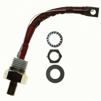
SILICON CONTROLLED RECTIFIER,2kV V(DRM),300A I(T),TO-209AE
Manufacturer
Vishay
Datasheet
1.ST300S12P0.pdf
(7 pages)
Specifications of ST300S20P0PBF
Scr Type
Standard Recovery
Voltage - Off State
2000V
Voltage - Gate Trigger (vgt) (max)
3V
Voltage - On State (vtm) (max)
1.66V
Current - On State (it (av)) (max)
300A
Current - On State (it (rms)) (max)
470A
Current - Gate Trigger (igt) (max)
200mA
Current - Hold (ih) (max)
600mA
Current - Off State (max)
50mA
Current - Non Rep. Surge 50, 60hz (itsm)
8000A, 8380A
Operating Temperature
-40°C ~ 125°C
Mounting Type
Chassis Mount
Package / Case
TO-209AE, TO-118
Current - On State (it (rms) (max)
470A
Breakover Current Ibo Max
8380 A
Rated Repetitive Off-state Voltage Vdrm
2000 V
Off-state Leakage Current @ Vdrm Idrm
50 mA
Forward Voltage Drop
1.66 V
Gate Trigger Voltage (vgt)
3 V
Maximum Gate Peak Inverse Voltage
5 V
Gate Trigger Current (igt)
200 mA
Holding Current (ih Max)
600 mA
Mounting Style
Stud
Maximum Operating Temperature
+ 125 C
Minimum Operating Temperature
- 40 C
Lead Free Status / RoHS Status
Lead free / RoHS Compliant
Other names
VS-ST300S20P0PBF
VS-ST300S20P0PBF
VSST300S20P0PBF
VSST300S20P0PBF
VS-ST300S20P0PBF
VSST300S20P0PBF
VSST300S20P0PBF


ST300SPbF Series
Vishay High Power Products
www.vishay.com
2
ABSOLUTE MAXIMUM RATINGS
PARAMETER
Maximum average on-state current
at case temperature
Maximum RMS on-state current
Maximum peak, one-cycle
non-repetitive surge current
Maximum I
Maximum I
Low level value of threshold voltage
High level value of threshold voltage
Low level value of on-state slope resistance
High level value of on-state slope resistance
Maximum on-state voltage
Maximum holding current
Typical latching current
SWITCHING
PARAMETER
Maximum non-repetitive rate of rise
of turned-on current
Typical delay time
Typical turn-off time
BLOCKING
PARAMETER
Maximum critical rate of rise of
off-state voltage
Maximum peak reverse and
off-state leakage current
2
2
t for fusing
√t for fusing
For technical questions, contact: ind-modules@vishay.com
SYMBOL
SYMBOL
SYMBOL
V
V
I
T(RMS)
dV/dt
I
I
I
I
T(TO)1
T(TO)2
V
dIdt
RRM
T(AV)
I
DRM
TSM
Phase Control Thyristors
I
2
r
r
t
t
I
I
2
TM
t1
t2
H
d
q
√t
L
t
(Stud Version), 300 A
,
Gate drive 20 V, 20 Ω, t
T
Gate current 1 A, dI
V
I
V
T
T
180° conduction, half sine wave
DC at 64 °C case temperature
t = 8.3 ms
t = 10 ms
t = 8.3 ms
t = 10 ms
t = 8.3 ms
t = 10 ms
t = 8.3 ms
t = 0.1 to 10 ms, no voltage reapplied
(16.7 % x π x I
(I > π x I
(16.7 % x π x I
(I > π x I
I
T
t = 10 ms
TM
pk
J
J
d
R
J
J
= T
= 0.67 % V
= T
= T
= 25 °C, anode supply 12 V resistive load
= 940 A, T
= 50 V, dV/dt = 20 V/µs, gate 0 V 100 Ω, t
= 550 A, T
J
J
J
maximum linear to 80 % rated V
maximum, anode voltage ≤ 80 % V
maximum, rated V
T(AV)
T(AV)
), T
), T
J
DRM
J
No voltage
reapplied
100 % V
reapplied
No voltage
reapplied
100 % V
reapplied
T(AV)
T(AV)
= T
= T
J
J
TEST CONDITIONS
TEST CONDITIONS
TEST CONDITIONS
= T
= T
, T
J
J
< I < π x I
< I < π x I
g
maximum, t
J
maximum, dI/dt = 40 A/µs,
/dt = 1 A/µs
J
J
= 25 °C
maximum
maximum
RRM
RRM
r
≤ 1 µs
DRM
T(AV)
T(AV)
Sinusoidal half wave,
initial T
/V
p
RRM
= 10 ms sine pulse
), T
), T
applied
J
J
J
= T
= T
= T
DRM
J
J
J
DRM
maximum
maximum
maximum
p
= 500 µs
Document Number: 94406
VALUES
VALUES
VALUES
Revision: 11-Aug-08
1000
8000
8380
6730
7040
3200
1000
0.97
0.98
0.74
0.73
1.66
500
300
470
320
292
226
207
600
100
1.0
30
75
UNITS
UNITS
UNITS
kA
kA
A/µs
V/µs
mA
mΩ
mA
µs
°C
A
A
V
V
2
2
√s
s
Related parts for ST300S20P0PBF
Image
Part Number
Description
Manufacturer
Datasheet
Request
R


Part Number:
Description:
357-036-542-201 CARDEDGE 36POS DL .156 BLK LOPRO
Manufacturer:
Vishay
Datasheet:
Part Number:
Description:
357-036-542-201 CARDEDGE 36POS DL .156 BLK LOPRO
Manufacturer:
Vishay
Datasheet:
Part Number:
Description:
357-036-542-201 CARDEDGE 36POS DL .156 BLK LOPRO
Manufacturer:
Vishay
Datasheet:
Part Number:
Description:
357-036-542-201 CARDEDGE 36POS DL .156 BLK LOPRO
Manufacturer:
Vishay
Datasheet:
Part Number:
Description:
357-036-542-201 CARDEDGE 36POS DL .156 BLK LOPRO
Manufacturer:
Vishay
Datasheet:
Part Number:
Description:
357-036-542-201 CARDEDGE 36POS DL .156 BLK LOPRO
Manufacturer:
Vishay
Datasheet:
Part Number:
Description:
357-036-542-201 CARDEDGE 36POS DL .156 BLK LOPRO
Manufacturer:
Vishay
Datasheet:
Part Number:
Description:
357-036-542-201 CARDEDGE 36POS DL .156 BLK LOPRO
Manufacturer:
Vishay
Datasheet:
Part Number:
Description:
357-036-542-201 CARDEDGE 36POS DL .156 BLK LOPRO
Manufacturer:
Vishay
Datasheet: